Multi-layer source/drain stressor

a stressor and multi-layer technology, applied in the field of integrated circuits, can solve problems such as reducing the stress being exerted

Inactive Publication Date: 2008-08-21
NORTH STAR INNOVATIONS
View PDF2 Cites 79 Cited by
  • Summary
  • Abstract
  • Description
  • Claims
  • Application Information

AI Technical Summary

Problems solved by technology

One of the difficulties is that the amount of stress being exerted is dependent on the germanium concentration but increasing the germanium concentration can cause the formation of defects which then causes a reduction in the stress being exerted.
In addition, as the device dimension shrinks during the technology evolution, one critical challenge is to maintain good performance characteristics for short channel transistors.

Method used


Image

  • Multi-layer source/drain stressor
  • Multi-layer source/drain stressor
  • Multi-layer source/drain stressor

Examples


Embodiment Construction

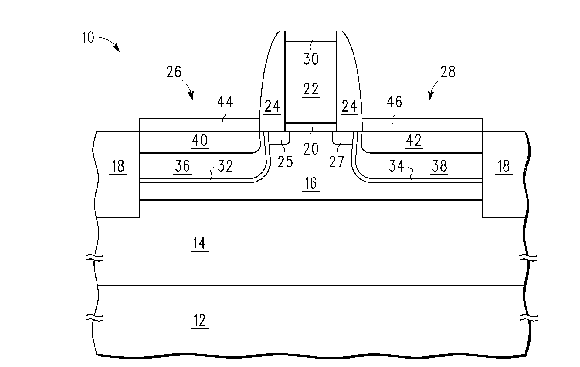
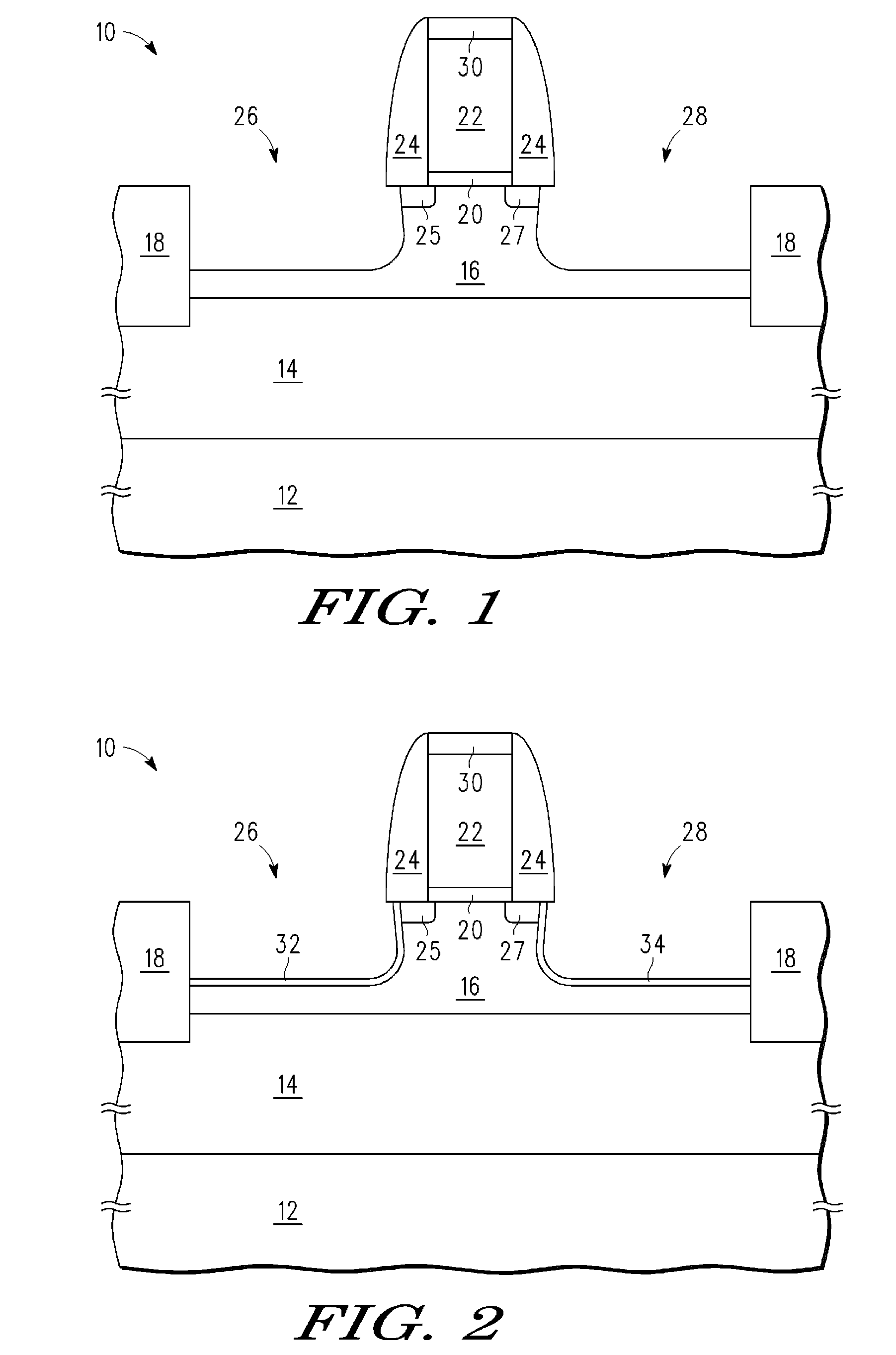
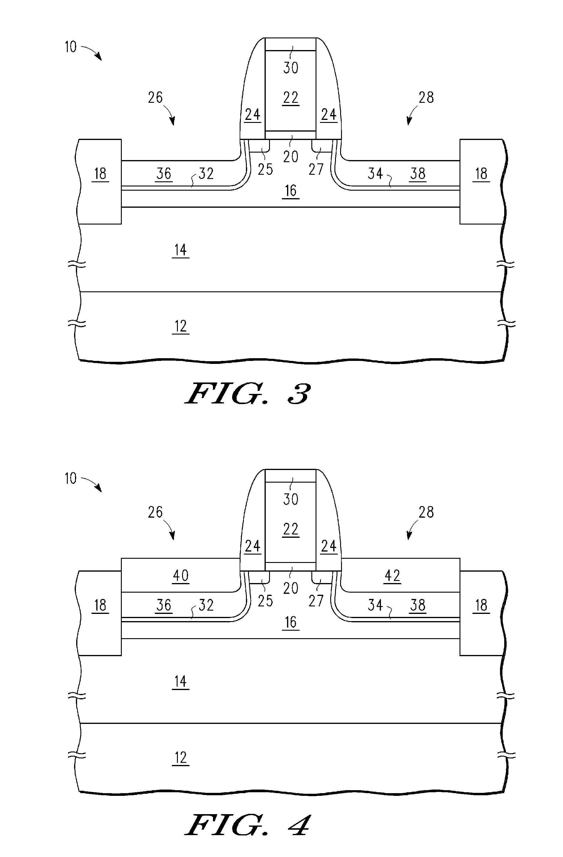
[0014]In one aspect, source / drains regions adjacent to a gate are removed and regrown using multiple layers of a different semiconductor combination. In one embodiment the semiconductor combination is an alloy of silicon and germanium (SiGe). The first layer has a first concentration of germanium and is doped with a first concentration of boron. Growth of the first layer is terminated before defects begin occurring. A first subsequent layer is grown at reduced germanium concentration which would not have defects until a second thickness is reached in which the second thickness is greater than the first thickness. The first subsequent layer is grown without defects and is boron-doped to a second concentration of boron greater than the first concentration of boron. A second subsequent layer is then grown at increased germanium concentration compared to the first subsequent layer and which is grown to a sufficiently low thickness so that there are substantially no defects. The boron do...


PUM


Abstract

A method for forming a semiconductor device includes forming a recess in a source region and a recess in a drain region of the semiconductor device. The method further includes forming a first semiconductor material layer in the recess in the source region and a second semiconductor material layer in the recess in the drain region, wherein each of the first semiconductor material layer and the second semiconductor material layer are formed using a stressor material having a first ratio of an atomic concentration of a first element and an atomic concentration of a second element, wherein the first element is silicon and a first level of concentration of a doping material. The method further includes forming additional semiconductor material layers overlying the first semiconductor material layer and the second semiconductor material layer that have a different ratio of the atomic concentration of the first element and the second element.

Description

BACKGROUND[0001]1. Field[0002]This disclosure relates generally to integrated circuits, and more specifically, to integrated circuits having a multi-layer source / drain stressor.[0003]2. Related Art[0004]One of the techniques for improving N channel and P channel transistor performance is by introducing strain to the channel. One of the techniques to introduce strain is to remove semiconductor material from the source / drain locations and regrowing a semiconductor material epitaxially which is of a different composition. For example, one approach for improving P channel performance, where the initial semiconductor material and thus the channel is just silicon, is regrowing a combination of silicon and germanium (SiGe) in the source / drain regions which exerts a compressive stress on the channel. One of the difficulties is that the amount of stress being exerted is dependent on the germanium concentration but increasing the germanium concentration can cause the formation of defects whic...

Claims


Application Information

Patent Timeline
Patent Type & Authority Applications(United States)
IPC IPC(8): H01L29/78H01L21/336
CPCH01L29/0847H01L29/165H01L29/7848H01L29/7834H01L29/66636H01L29/66348
Inventor ZHANG, DADHANDAPANI, VEERARAGHAVANGOEDEKE, DARREN V.HILDRETH, JILL C.
Owner NORTH STAR INNOVATIONS
Why Eureka
Try Eureka