Display panel, method for manufacturing the same, motherboard for manufacturing the same and method for manufacturing a display substrate for the same

a technology for display panels and motherboards, which is applied in the direction of electrical devices, semiconductor devices, instruments, etc., can solve the problems of metal corroding in contact holes, and achieve the effects of preventing the separation of the first substrate and the second substrate, reducing the defect caused by static charge generated during the manufacturing process, and preventing the corrosion of the gate driving par

Active Publication Date: 2008-08-21
SAMSUNG DISPLAY CO LTD
View PDF6 Cites 21 Cited by
  • Summary
  • Abstract
  • Description
  • Claims
  • Application Information

AI Technical Summary

Benefits of technology

[0017]According to the display panel and a method for manufacturing a display substrate, separation of the first substrate and the second substrate may be prevented. Also, corrosion of the gate driving part may be prevented. In addition, defects caused by static charge generated during processes for manufacturing the first substrate may be decreased.

Problems solved by technology

In addition, since the gate driver includes a plurality of areas in which a gate metal is in contact with a data metal, the metal may corrode in contact holes, through which the gate metal is in contact with the data metal.

Method used


Image

  • Display panel, method for manufacturing the same, motherboard for manufacturing the same and method for manufacturing a display substrate for the same
  • Display panel, method for manufacturing the same, motherboard for manufacturing the same and method for manufacturing a display substrate for the same
  • Display panel, method for manufacturing the same, motherboard for manufacturing the same and method for manufacturing a display substrate for the same

Examples


Embodiment Construction

[0025]The invention is described more fully hereinafter with reference to the accompanying drawings, in which exemplary embodiments of the invention are shown. This invention may, however, be embodied in many different forms and should not be construed as limited to the embodiments set forth herein.

[0026]It will be understood that when an element or layer is referred to as being “on,”“connected to” or “coupled to” another element or layer, it can be directly on, connected or coupled to the other element or layer or intervening elements or layers may be present.

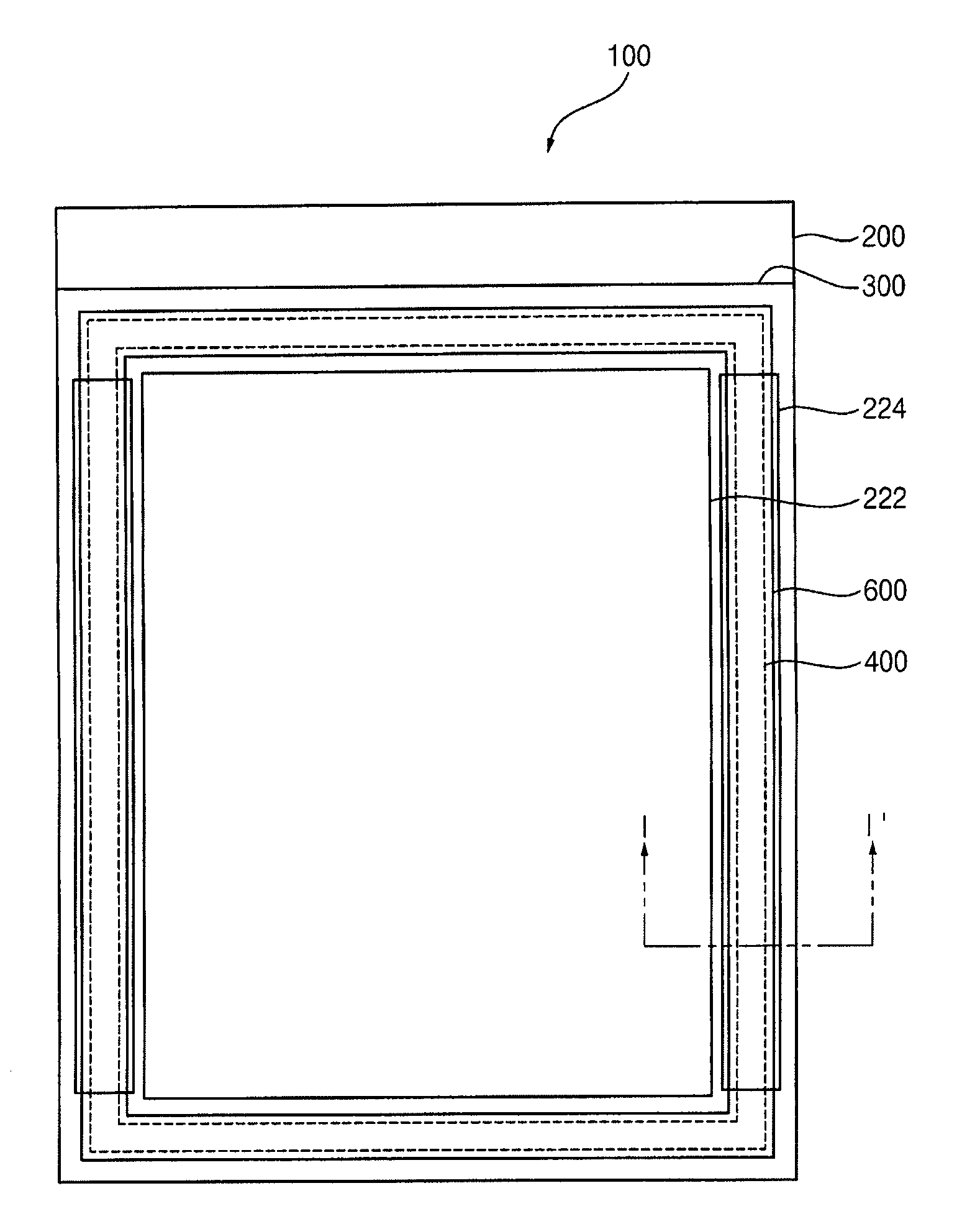
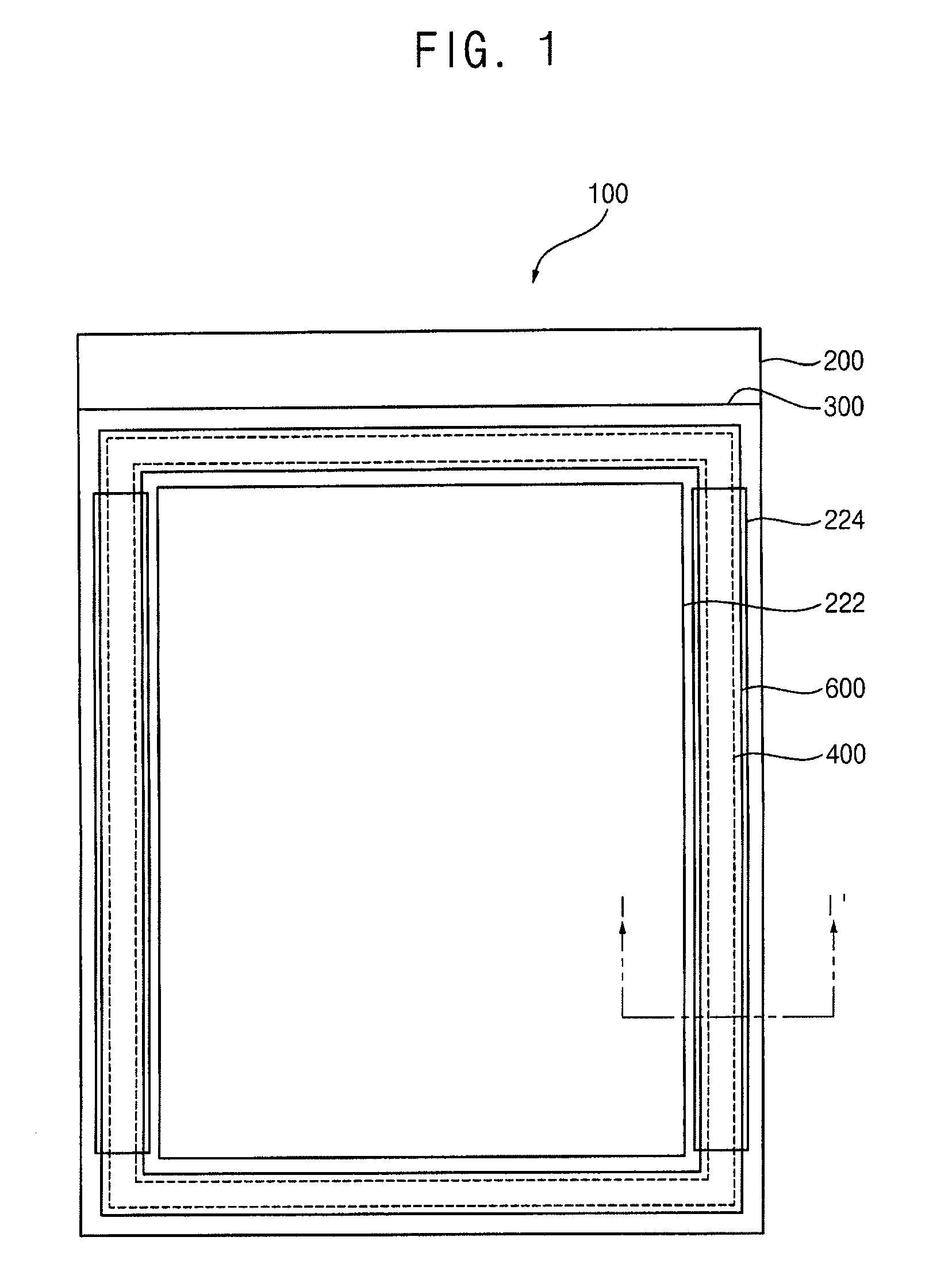
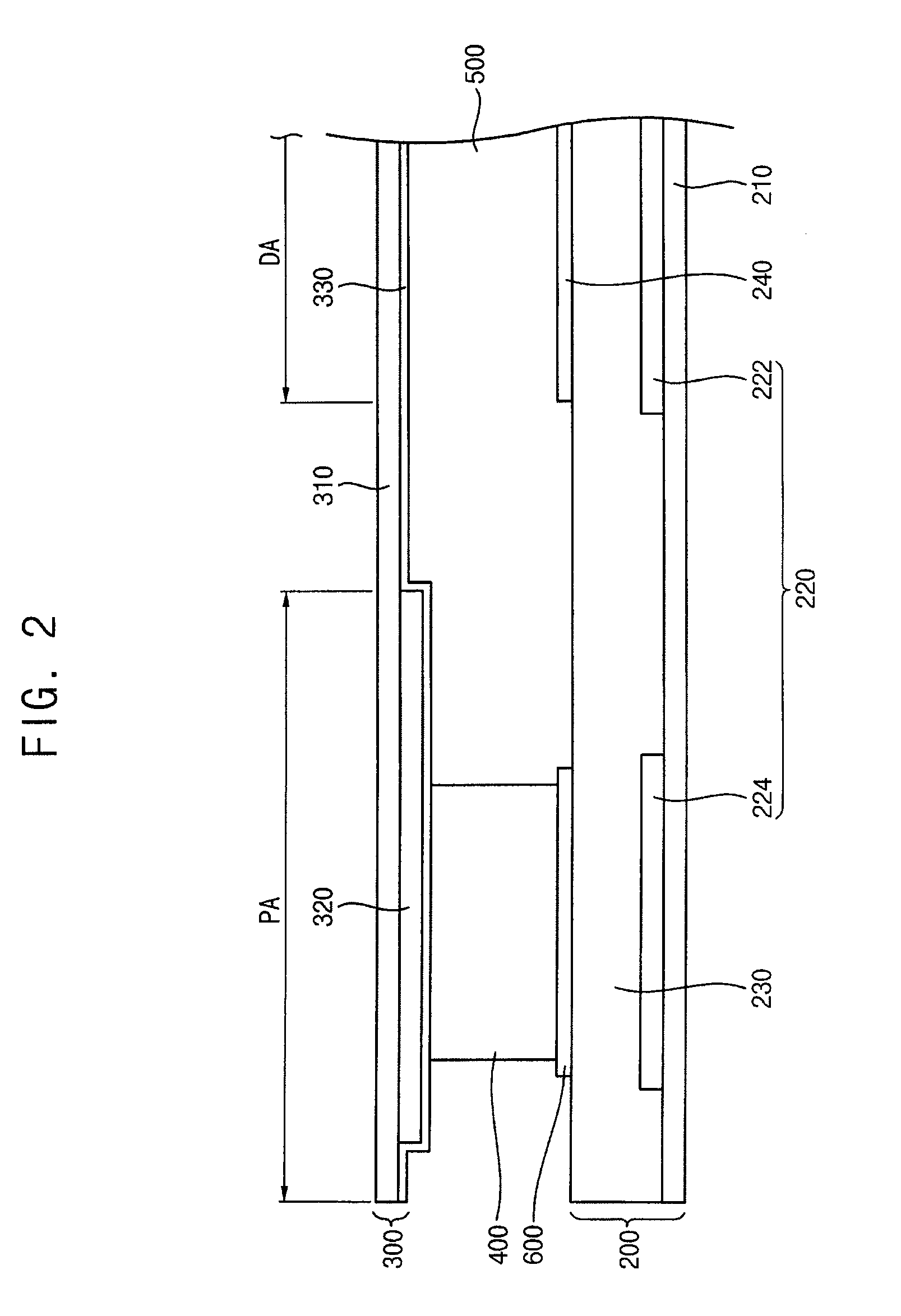
[0027]FIG. 1 is a plan view illustrating a display panel according to an exemplary embodiment of the present invention. FIG. 2 is a cross-sectional view taken along a line I-I′ shown in FIG. 1.

[0028]Referring to FIGS. 1 and 2, a display panel 100 includes a first substrate 200, a thin-film transistor (TFT) 220, an organic layer 230, a seal line 400, and a conductive pattern 600.

[0029]The display panel 100 includes a display ar...


PUM

PropertyMeasurementUnit
DAaaaaaaaaaa
thicknessaaaaaaaaaa
widthaaaaaaaaaa

Abstract

A display panel includes a first substrate, a thin-film transistor (TFT), an organic layer, a second substrate, a seal line, and a conductive pattern. The first substrate includes a pixel part and a driving part connected to the pixel part. The TFTs are formed in the pixel part and the driving part. The organic layer is formed on the first substrate having the TFTs formed thereon. The second substrate is opposite to the first substrate. The seal line is disposed between an edge portion of the first substrate having the organic layer formed thereon and an edge portion of the second substrate. The seal line combines the first substrate with the second substrate. The conductive pattern is disposed between the seal line and the organic layer.

Description

CROSS-REFERENCE TO RELATED APPLICATION[0001]This application claims priority under 35 U.S.C. §119 to Korean Patent Application No. 2007-16893, filed on Feb. 20, 2007 in the Korean Intellectual Property Office (KIPO), the contents of which are herein incorporated by reference in their entirety.BACKGROUND OF THE INVENTION[0002]1. Technical Field[0003]The present invention relates to a display panel, a method for manufacturing the display panel, a motherboard for manufacturing the display panel, and a method for manufacturing a display substrate for the display panel.[0004]2. Discussion of the Related Art[0005]A display panel displaying an image includes a first substrate, a second substrate facing the first substrate and a liquid crystal layer interposed between the first substrate and the second substrate. The first substrate includes a thin-film transistor (TFT) formed in each pixel to independently drive the pixel.[0006]The display panel includes a display area displaying the image...

Claims


Application Information

Patent Timeline
Patent Type & Authority Applications(United States)
IPC IPC(8): H01L21/70H01L27/02G02F1/1368
CPCG02F1/1339G02F2202/02G02F2001/133357G02F1/13454G02F1/133357
Inventor KIM, HYUN-YOUNGJUNG, KWAN-WOOKNA, HYUNG-DONTAE, SEUNG-GYUKIM, JUNG-YUN
Owner SAMSUNG DISPLAY CO LTD
Why Eureka
Try Eureka