Power Semiconductor Module

a technology of semiconductor modules and semiconductor components, applied in the direction of printed circuit manufacturing, printed circuit aspects, laminated printed circuit boards, etc., can solve the problems of device damage or device characteristics degradation, difficulty in making the coefficient of thermal expansion of materials above and below the device equal, and fracture of the joining part, so as to prevent the fracture of the joining parts, reduce the possibility of device damage, and reduce the effect of pressur

Inactive Publication Date: 2007-11-22
HITACHI LTD
View PDF3 Cites 40 Cited by
  • Summary
  • Abstract
  • Description
  • Claims
  • Application Information

AI Technical Summary

Benefits of technology

[0013]Between the ceramic substrates with printed circuit, an insulating inorganic material having a coefficient of thermal expansion equivalent to that of the device is disposed besides the power semiconductor device. Therefore, the space filled with resin when filling the space between the ceramic substrates with printed circuit with the resin becomes small. When the temperature of the power semiconductor module has become high, therefore, force pushing up the ceramic substrate with printed circuit because of expansion of the resin is weakened. As a result, the joining part of the device is prevented from being fractured. On the other hand, when the temperature at the power semiconductor module has become low, pushing pressure exerted from the external cooling substances is supported by the inorganic material. Therefore, the pressure is dispersed and the possibility that the device will be damaged can be reduced.
[0014]In addition, in the structure in which the inorganic material is joined to the upper and lower ceramic substrates with printed circuit, the joining part of the device and the joining part of the inorganic material take partial charge of the force pushing up the ceramic substrate with printed circuit when the resin is expanded. As a result, the tensile strain applied to each joining part becomes small and it becomes possible to prevent joining parts from being fractured.
[0015]According to the present invention, the low thermal expansion ceramic substrates are disposed above and blow the power semiconductor device and a low thermal expansion material having a coefficient of thermal expansion of 10 ppm / K or less is disposed between the substrates. Even when the temperature at the power semiconductor module in use has become a high temperature in the range of 175 to 250° C., therefore, warp deformation of the power semiconductor module having a power device joined to and mounted on the ceramic substrate with printed circuit is prevented. It is thus possible to provide a power semiconductor module capable of remarkably improving the thermal fatigue life by reducing the thermal strain generated in the joining part of the power device, and capable of maintaining high cooling performance by ensuring close adhesion between the ceramic substrate with printed circuits and the cooling substances.
[0016]In addition, an inorganic material having a coefficient of thermal expansion in the range of 2 to 6 ppm / K is disposed around the device. As for a power semiconductor module obtained by interposing the power semiconductor device between the ceramic substrates with printed circuit and joining the electrode of the power device to the electrodes on ceramic substrate with printed circuit, therefore, it is possible to provide a highly reliable power semiconductor module in which the thermal strain in the tensile direction applied to the joining part of the power device is reduced even when the temperature at the power semiconductor module in use has become a high temperature in the range of 170 to 250° C. and the pushing pressure generated onto the power device by the cooling substance is reduced.

Problems solved by technology

In addition, it is difficult to make coefficients of thermal expansion of the materials above and below the device equal to each other.
The thermal stress occurs repeatedly at the time of operation of the power device, resulting in a problem of fracture of the joining part caused by thermal fatigue.
If warp deformation occurs, close adhesion between the insulating plate and the cooling substance is worsened and the cooling performance is lowered, resulting in a problem of a device damage or device characteristics degradation caused by the raised power device temperature.
If the temperature of the power semiconductor module becomes a high temperature in the range of 175 to 250° C. higher than 150° C. which is the setting temperature of the resin, then force that widens the insulating substrates vertically is generated by expansion of the resin, resulting in a problem of fracture of the joining part caused by great tensile strength generated in the joining parts between the power device and the upper and lower electrodes on ceramic substrate with printed circuit.
In the structure obtained by disposing the cooling substances above and below the power semiconductor module for the purpose of both side cooling and pushing the cooling substances against the upper and lower high thermal conductive insulating substrates to ensure the cooling performance, the material that supports the pushing pressure at the time of low temperature becomes only the power device and strain concentrates thereon, resulting in a problem that the circuit face side of the power device having a small joining area is susceptible to mechanical damage.
In this case, especially the problem of the pushing pressure applied to the device becomes remarkable.
If the pushing pressure is made low, then mechanical damage can be prevented, but another problem that the cooling performance remarkably falls is posed.

Method used


Image

  • Power Semiconductor Module
  • Power Semiconductor Module
  • Power Semiconductor Module

Examples


Embodiment Construction

[0025]Hereafter, embodiments of the present invention will be described in detail with reference to the drawings.

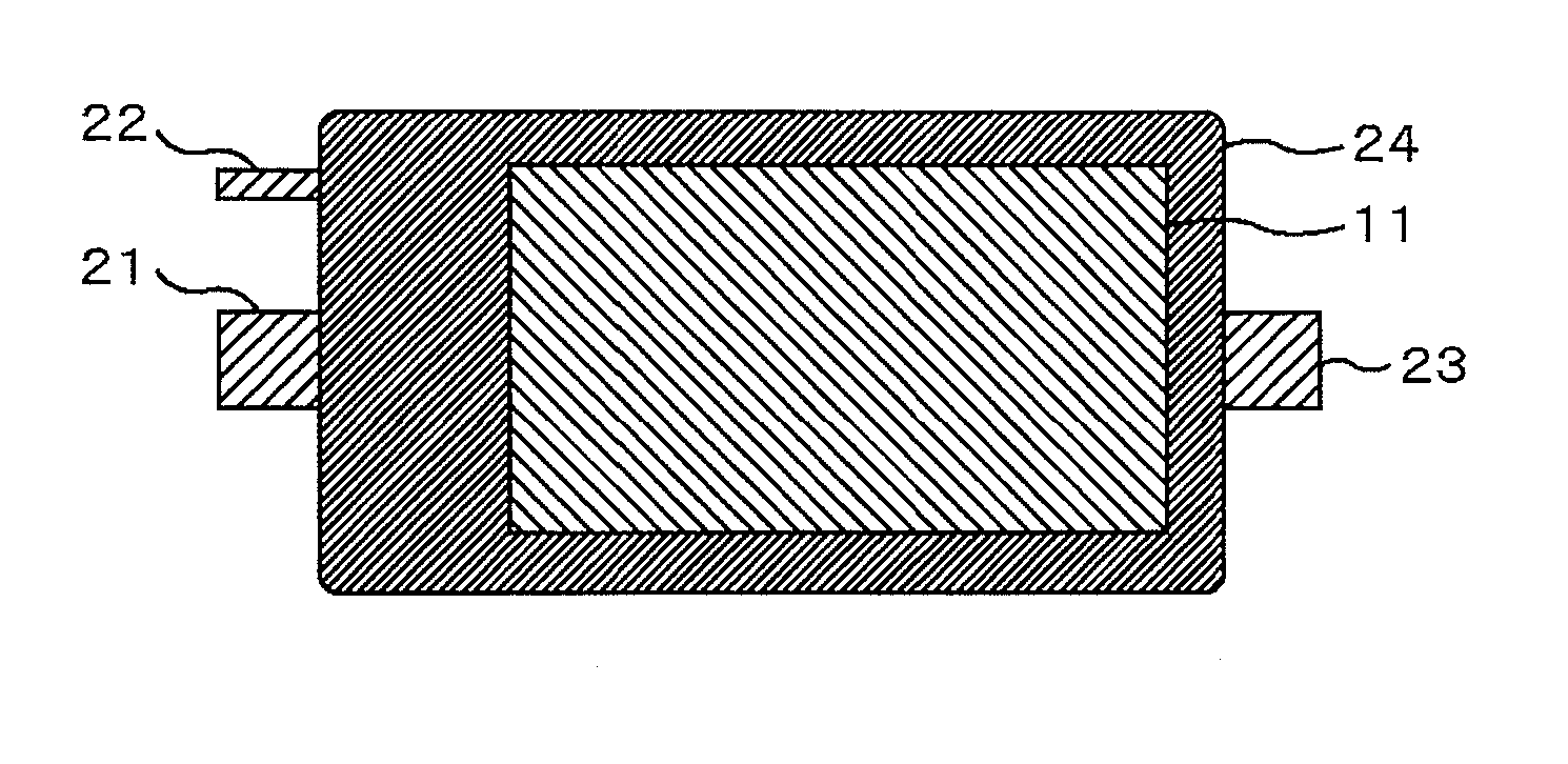
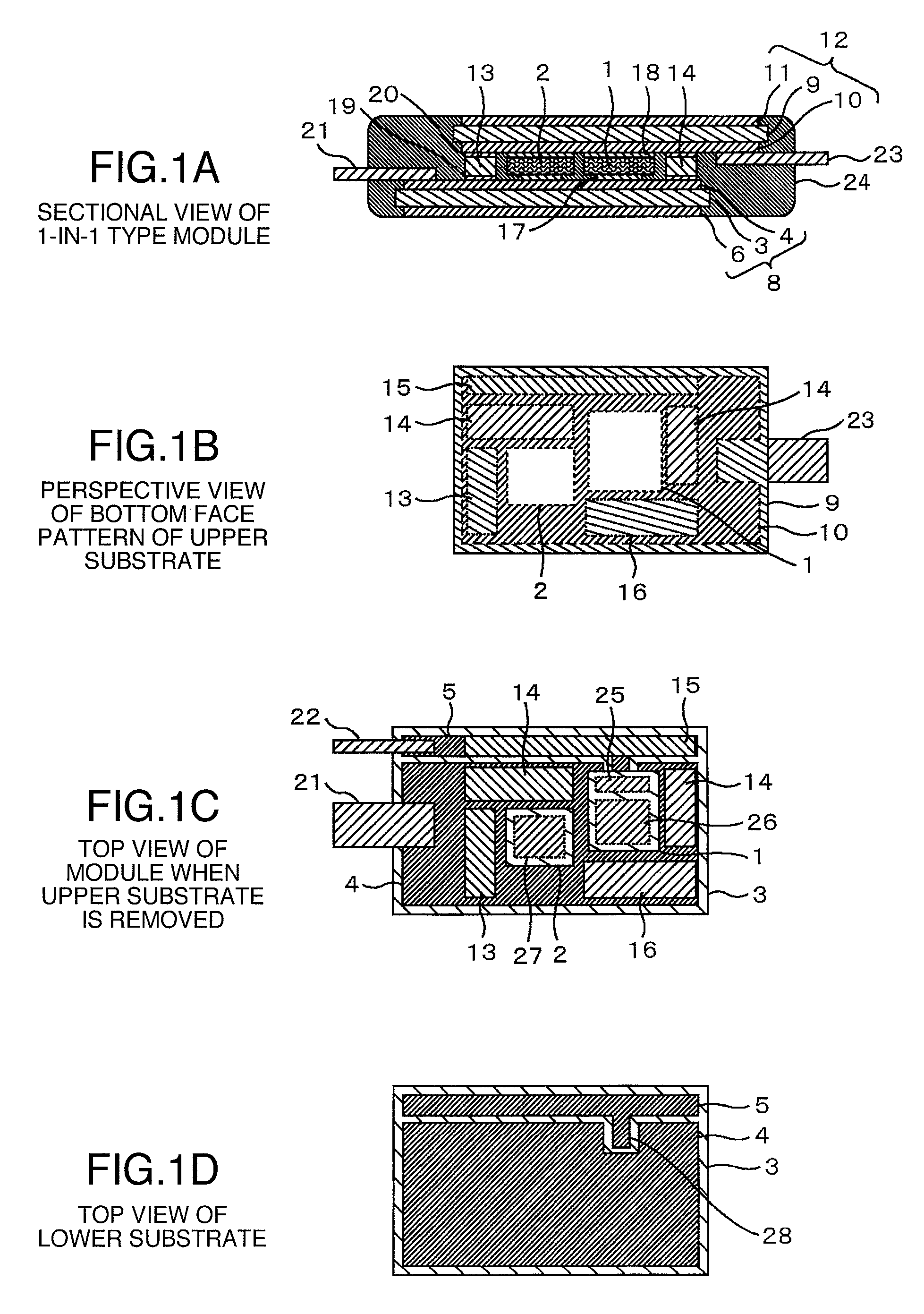
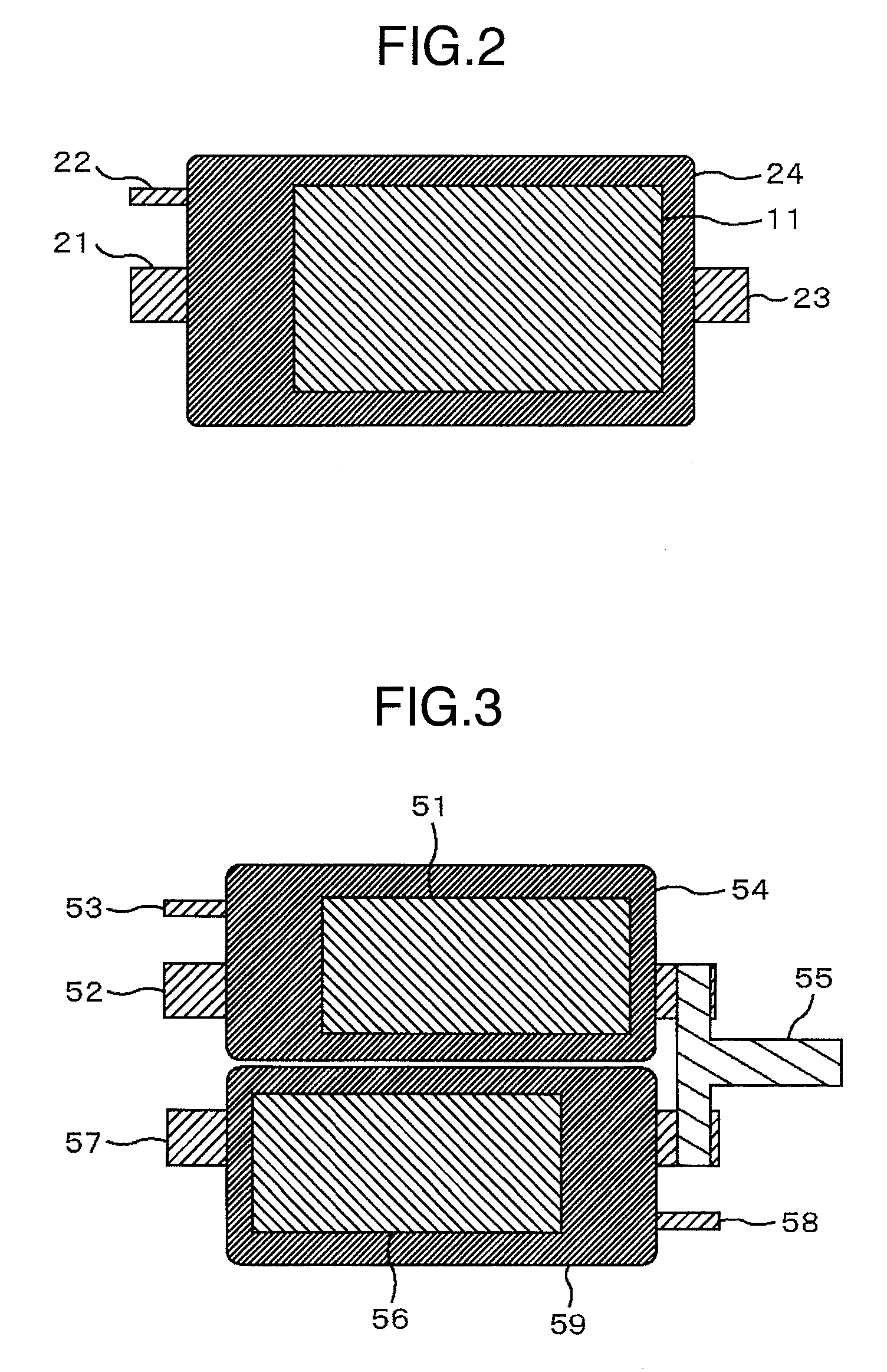
[0026]FIGS. 1A-1D show an embodiment of a power semiconductor module according to the present invention including one power transistor device and one diode device. FIG. 1A is a sectional view of the module. FIG. 1B is a perspective view of a metal electrode of a device side face on an upper ceramic substrate with printed circuit. FIG. 1C is a top view obtained when an upper substrate with printed circuit and resin are removed. FIG. 1D is a top view of a lower substrate with printed circuit. In FIGS. 1A-1D, an IGBT chip 1 and a diode chip 2 are joined onto a ceramic substrate with printed circuit 8 having metal electrodes 4, 5 and 6 of Cu formed above and below a low thermal expansion ceramic substrate 3 with printed circuit, by high temperature solder 17 having a temperature at solidus line of at least 260° C. formed of SnSbAgCu. Electroless Ni—P plating having a thicknes...


PUM

PropertyMeasurementUnit
melting pointaaaaaaaaaa
temperatureaaaaaaaaaa
thicknessaaaaaaaaaa

Abstract

A power semiconductor module and an inverter apparatus in which a device or a joining part is not mechanically damaged even when the temperature in use becomes a high temperature in the range of 175 to 250° C., resulting in excellent reliability at high temperature retaining test and thermal cycling test. Low thermal expansion ceramic substrates are disposed above and below the device. A material having a coefficient of thermal expansion of 10 ppm/K or less is disposed between the ceramic substrates. In addition, an inorganic material having a coefficient of thermal expansion in the range of 2 to 6 ppm/K or less is disposed around the device.

Description

BACKGROUND OF THE INVENTION[0001]The present invention relates to a large current control semiconductor device used in high temperature environments represented by use in automobiles. In particular, the present invention relates to a power semiconductor module that is excellent in heat resistance of its junction and constituent materials and excellent in thermal fatigue life against the thermal cycling test or the power cycling test caused by the on / off of the device, even in the case where operation is conducted with the junction temperature of the semiconductor device in the range of 175 to 250° C.[0002]Power semiconductor modules including power devices, such as MOSFETs and IGBTs, for exercising switching control on a large current and diodes for releasing the reverse voltage generated at the time of switching are used in wide fields ranging from household electric appliances to vehicles as main components of inverter apparatuses for power converter. In recent years, motor contro...

Claims


Application Information

Patent Timeline
Patent Type & Authority Applications(United States)
IPC IPC(8): H01L23/34
CPCH01L23/16H01L24/33H01L23/4334H01L23/49575H01L23/49844H01L23/5385H01L25/072H01L2924/13055H01L2924/13091H05K1/0306H05K3/0058H05K3/284H05K2201/0715H05K2201/10166H01L2224/32225H01L2224/33181H01L23/3735H01L2924/15787H01L2924/181H01L2924/351H01L2924/00H01L2924/00012
Inventor KAJIWARA, RYOICHISUZUKI, KAZUHIROISHII, TOSHIAKIITOU, KAZUTOSHI
Owner HITACHI LTD
Why Eureka
Try Eureka