
Eureka
For R&D, Eureka makes reading and utilizing patents & technical documents easy.
Eureka AIR
Designed for self-driven R&D workflows. Generate viable solutions, solve complex R&D challenges, empower your innovation with AI.

Eureka Materials
Designed for material experts only. Revolutionize your material R&D, from search, analyze, to developing new materials.

TechResearch
Generate reliable direction feasibility study reports for your R&D in just a few steps.

TechSeek
Discover and master advanced knowledge NOW. Basics, ideas, possibilities, all at once.

TechMind
As an expert in R&D Theories, TechMind can generates customized viable solutions instantly.

TechRisk
Analyze your overall solution with one click, know your potential R&D risks in advance.

TechMonitor
Get weekly tech updates, stay abreast of the latest tech innovations and key insights.
Power supply control circuit
- Summary
- Abstract
- Description
- Claims
- Application Information
AI Technical Summary
Benefits of technology
Problems solved by technology
Method used
Image

Examples
embodiment 1
Preferred Embodiment 1
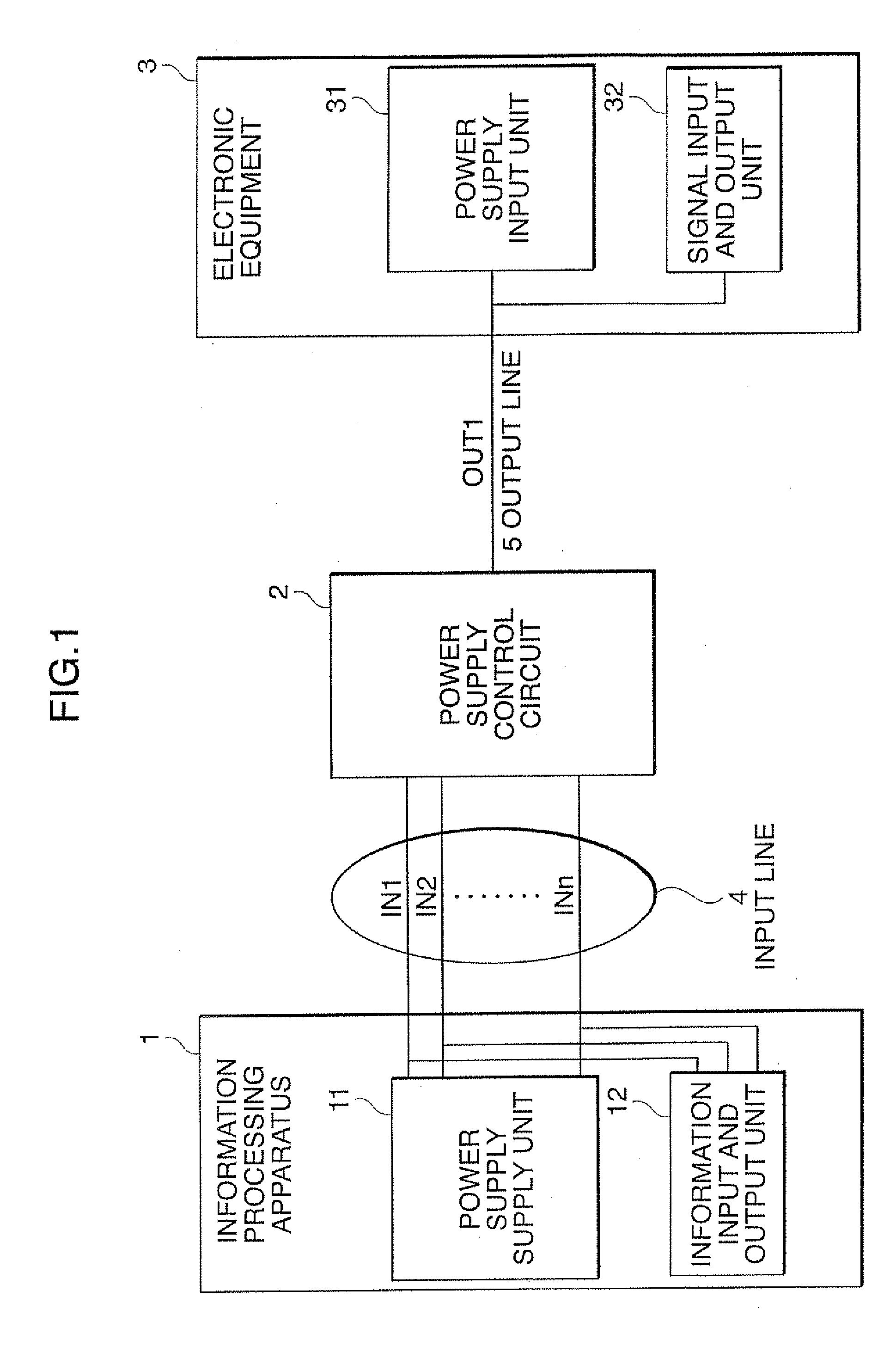
[0132]FIG. 6 is a diagram for describing a preferred embodiment 1 of a power supply control circuit according to the present invention. In this case, there is shown a case where two input lines are connected as in FIG. 2 or the like.
[0133]In FIG. 6, one of two input lines is a USB cable to be connected to a USB terminal (USB1) of an information processing apparatus 1. The other input line is a power supply line to be connected to a USB2 terminal of the information processing apparatus 1.
[0134]The USB cable includes two signal lines (D+ and D−) (not shown in the drawing), and two power supply supply lines (Vbus and GND). The input line to be connected to a DCjack includes a Vcc line and a GND line. In FIG. 6, the USB cable or a USB power supply auxiliary cable is used.
[0135]An FET 22 and a diode D1 shown in FIG. 2 or the like are connected in parallel in the Vbus line of the USB cable.
[0136]In this case, a P channel FET (Pch FET) is used for the FET 22.
[0137]An ...
embodiment 2
Preferred Embodiment 2
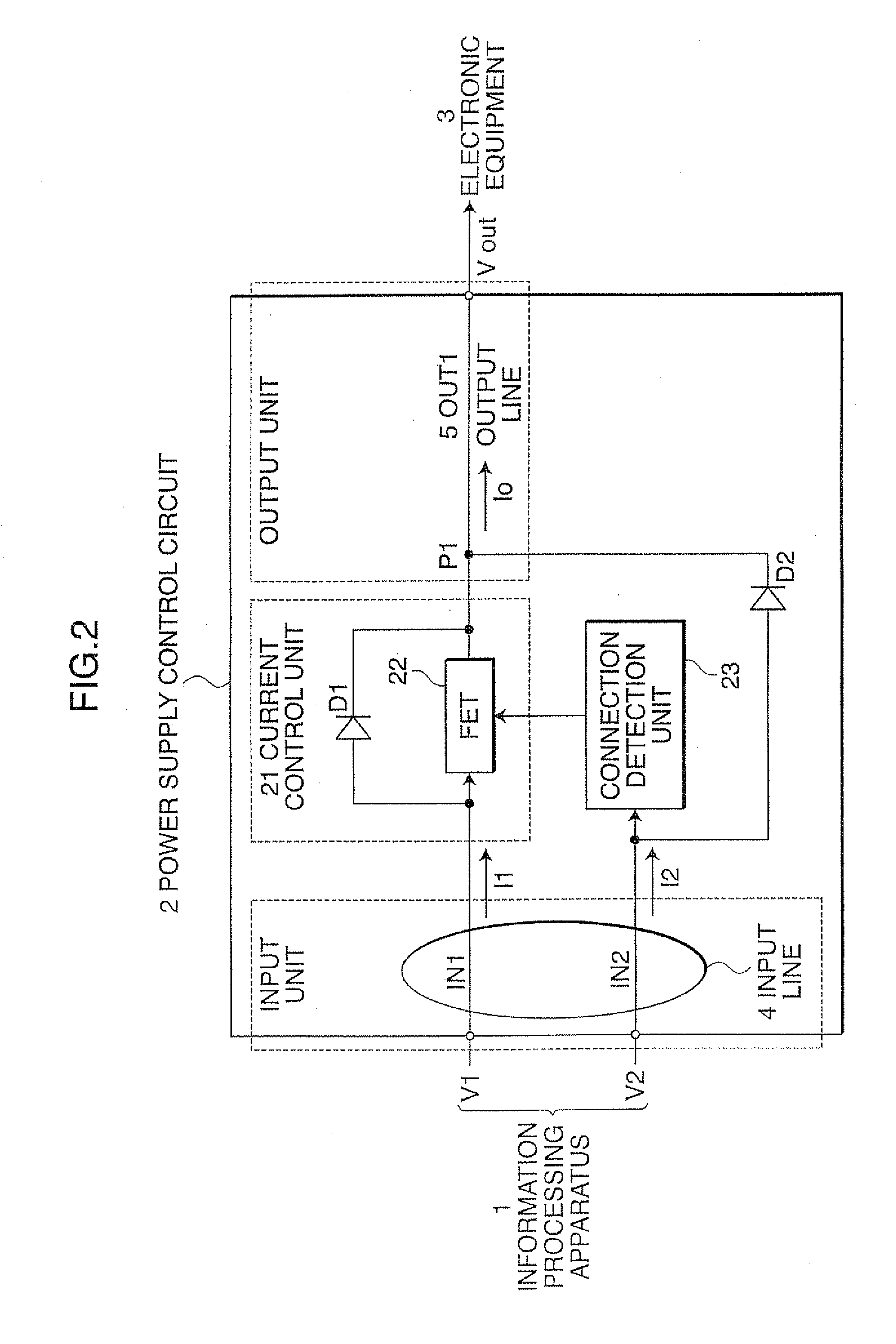
[0152]In this case, there is described a preferred embodiment in a case where a diode D2 is not provided in a power supply control circuit 2.
[0153]As described before, the power supply control circuit 2 is a circuit adopted in a case where a voltage V2 which is supplied to an input line IN2 connected to a connection detection unit 23 is the same or higher (V2≧V1) than a voltage V1 which is supplied to an input line IN1 connected to a current control unit 21.
[0154]FIG. 7 is a block diagram showing a preferred embodiment 2 of a power supply control circuit according to the present invention.
[0155]In this case, it is different from FIG. 2 in that the diode D2 is not provided. In this regard, however, it is set to the voltage V2 of the input line IN2≧the voltage V1 of the input line IN1.
[0156]FIG. 8 is a diagram for describing a specific example of the preferred embodiment 2 of the power supply control circuit according to the present invention.
[0157]In this case, ...
embodiment 3
Preferred Embodiment 3
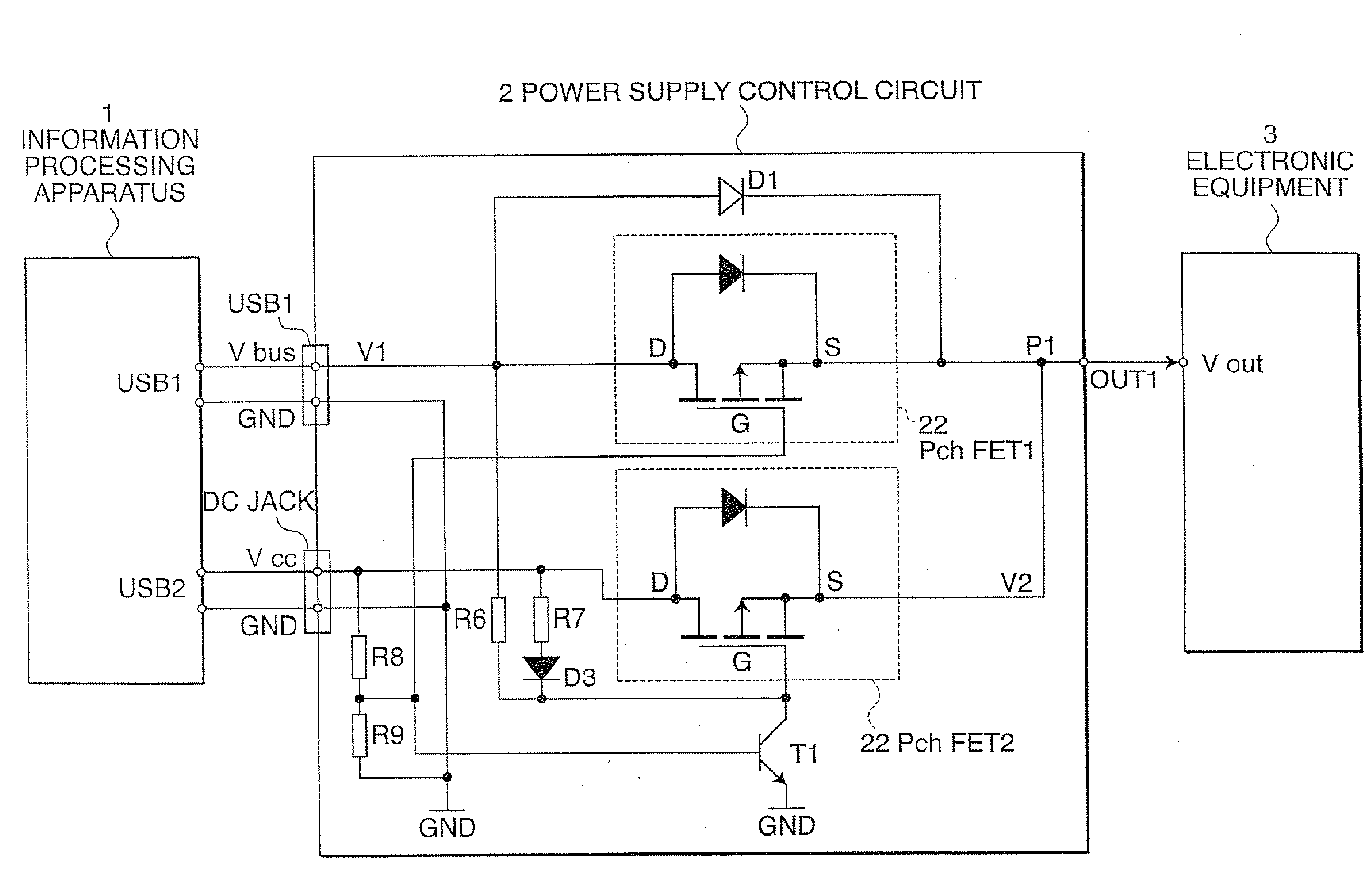
[0174]FIG. 10 is a diagram for describing a preferred embodiment 3 of a power supply control circuit according to the present invention.
[0175]The preferred embodiment 3 is also conditional on that a voltage V2 supplied to a Vcc of a DCjack is higher than a voltage V1 supplied to a Vbus of a USB (V2≧V1), and a diode D2 is not provided as in the preferred embodiment 2.
[0176]In FIG. 10, a Pch FET2, four resistors (R6 to R9), a transistor T1, and a diode D3 are provided at a section corresponding to the connection detection unit 23 shown in FIG. 7.
[0177]A Pch FET1 and a diode D1 connected to the Vbus are the same as those shown in FIG. 2, FIG. 6, and FIG. 7; and an operation for supplying a power supply are also the same.
[0178]In FIG. 10, two FETs 22 are a P channel type FET having the same characteristic, a drain D is arranged on the input line side, and a source S is arranged on the output line side.
[0179]First, an operation in a case where a USB cable is connect...
PUM
 Abstract
Description
Claims
Application Information
 - R&D Engineer
- R&D Manager
- IP Professional
- Industry Leading Data Capabilities
- Powerful AI technology
- Patent DNA Extraction
Browse by: Latest US Patents, China's latest patents, Technical Efficacy Thesaurus, Application Domain, Technology Topic, Popular Technical Reports.
© 2024 PatSnap. All rights reserved.Legal|Privacy policy|Modern Slavery Act Transparency Statement|Sitemap|About US| Contact US: help@patsnap.com