Methods of manufacturing non-volatile memory devices by implanting metal ions into grain boundaries of variable resistance layers, and related devices

a non-volatile memory and metal ion technology, applied in the direction of filtration separation, separation process, chemical apparatus and processes, etc., can solve the problems of deteriorating the reproducibility of manufacturing the non-volatile memory device, different resistances of the node, etc., and achieve the effect of improving the operation characteristics of the resistive non-volatile memory devi

Active Publication Date: 2008-08-28
SAMSUNG ELECTRONICS CO LTD
View PDF4 Cites 40 Cited by
  • Summary
  • Abstract
  • Description
  • Claims
  • Application Information

AI Technical Summary

Benefits of technology

[0027]According to various embodiments of the present invention, the metal filaments can be formed uniformly along the grain boundaries in the variable resistance material layer pattern by a metal ion implantation. Thus,...

Problems solved by technology

Unfortunately, however, the resistance nodes may have different resistances.
Further, performing several processes for c...

Method used


Image

  • Methods of manufacturing non-volatile memory devices by implanting metal ions into grain boundaries of variable resistance layers, and related devices
  • Methods of manufacturing non-volatile memory devices by implanting metal ions into grain boundaries of variable resistance layers, and related devices
  • Methods of manufacturing non-volatile memory devices by implanting metal ions into grain boundaries of variable resistance layers, and related devices

Examples


Embodiment Construction

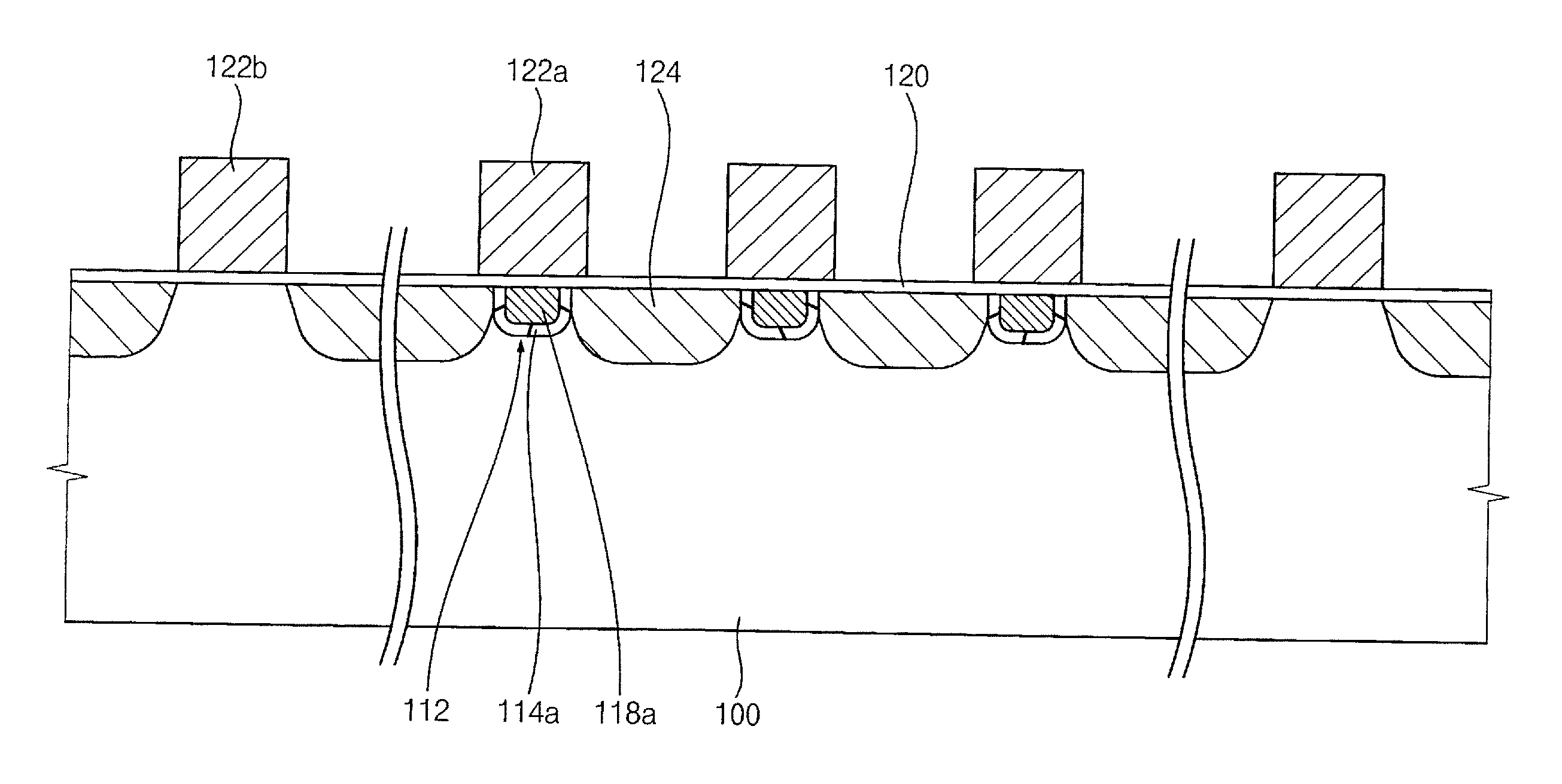
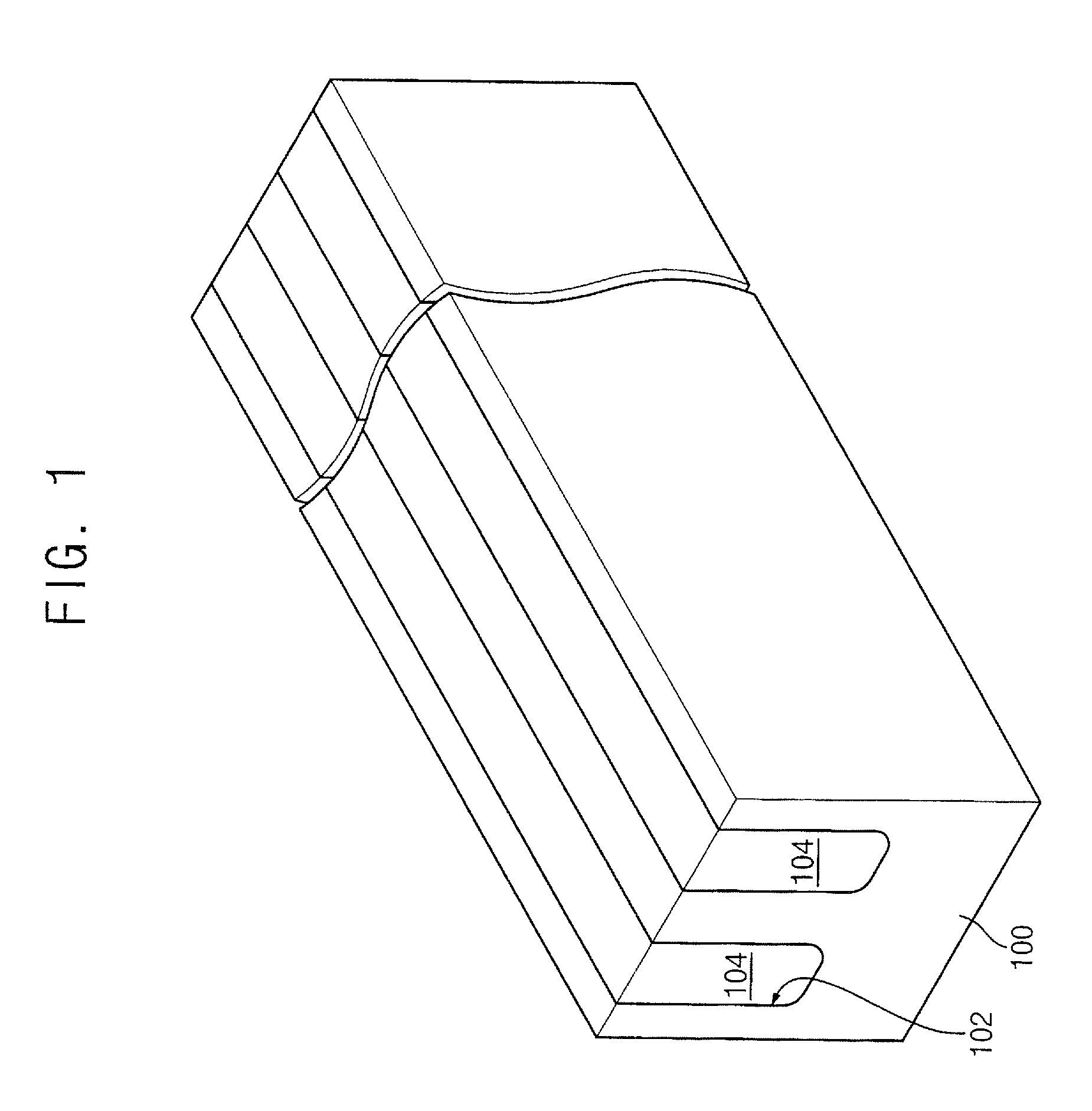
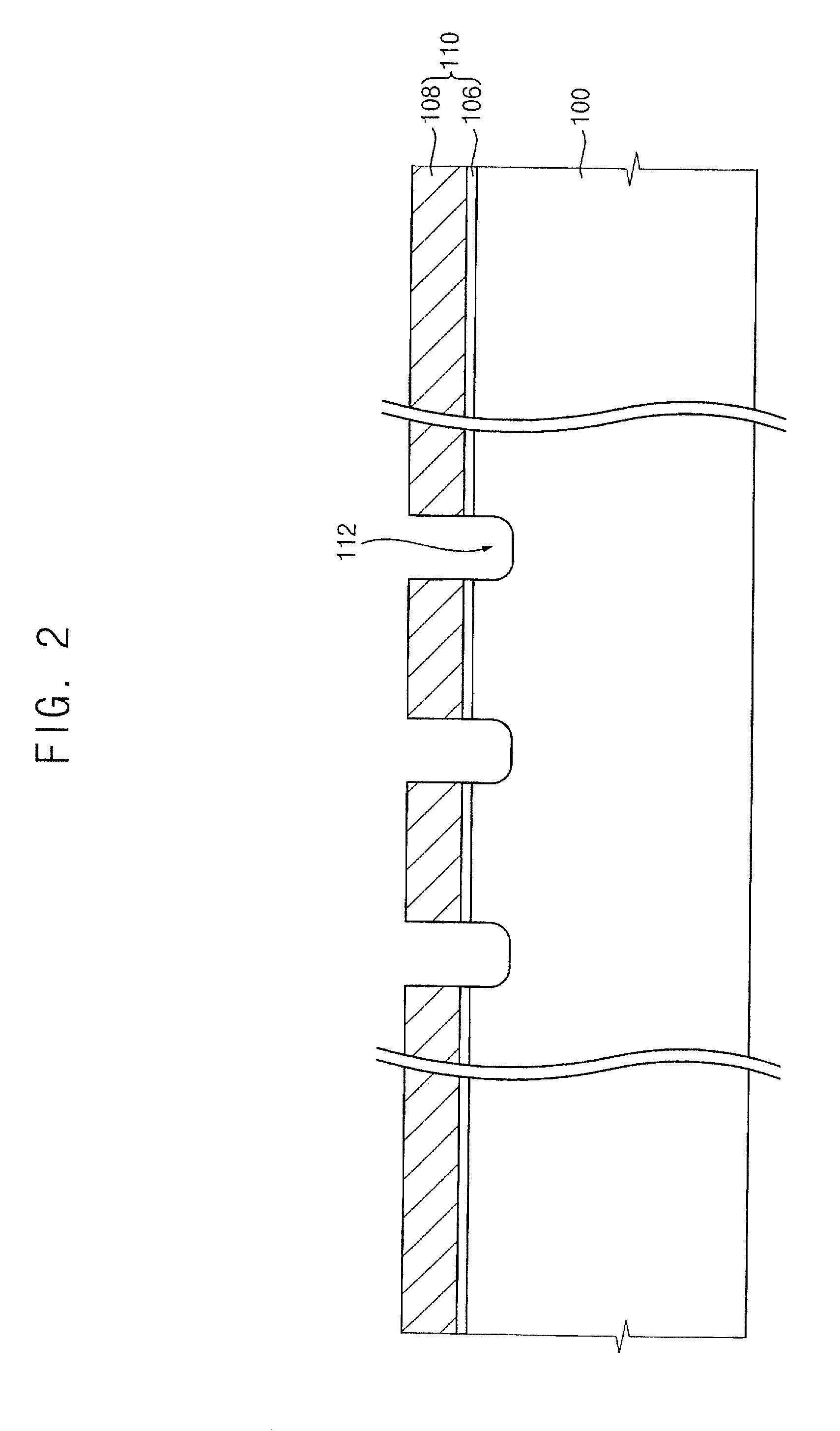
[0035]The present invention is described more fully hereinafter with reference to the accompanying drawings, in which embodiments of the present invention are shown. The present invention may, however, be embodied in many different forms and should not be construed as limited to the embodiments set forth herein. Rather, these embodiments are provided so that this disclosure will be thorough and complete, and will fully convey the scope of the present invention to those skilled in the art. In the drawings, the sizes and relative sizes of layers and regions may be exaggerated for clarity.

[0036]It will be understood that when an element or layer is referred to as being “on,”“connected to” or “coupled to” another element or layer, it can be directly on, connected or coupled to the other element or layer or intervening elements or layers may be present. In contrast, when an element is referred to as being “directly on,”“directly connected to” or “directly coupled to” another element or l...


PUM

PropertyMeasurementUnit
Electrical resistanceaaaaaaaaaa
Electrical conductoraaaaaaaaaa
Grain boundaryaaaaaaaaaa

Abstract

Integrated circuit nonvolatile memory devices are manufactured by forming a variable resistance layer on an integrated circuit substrate. The variable resistance layer includes grains that define grain boundaries between the grains. Conductive filaments are formed along at least some of the grain boundaries. Electrodes are formed on the variable resistance layer. The conductive filaments may be formed by implanting conductive ions into at least some of the grain boundaries. Moreover, the variable resistance layer may be a variable resistance oxide of a metal, and the conductive filaments may be the metal. Related devices are also disclosed.

Description

CROSS-REFERENCE TO RELATED APPLICATION[0001]This application claims the benefit under 35 U.S.C. §119 to Korean Patent Application No. 10-2007-0019826, filed on Feb. 27, 2007, the disclosure of which is hereby incorporated herein by reference in its entirety as if set forth fully herein.FIELD OF THE INVENTION[0002]The present invention relates to methods of manufacturing integrated circuit non-volatile memory devices. More particularly, the present invention relates to methods of manufacturing integrated circuit non-volatile memory devices including a material whose resistance varies according to an applied voltage, and related devices.BACKGROUND OF THE INVENTION[0003]Generally, non-volatile memory devices may be classified as either floating-gate type memory devices or charge-trap type memory devices in accordance with a structure of a unit cell incorporated therein.[0004]The unit cell of a typical floating-gate type non-volatile memory device includes a tunnel oxide layer, a floati...

Claims


Application Information

Patent Timeline
IPC IPC(8): H01L47/00
CPCH01L27/2436H01L45/085H01L45/165H01L45/146H01L45/1226H10B63/30H10N70/245H10N70/253H10N70/823H10N70/8833H10N70/043B01D39/08B01D46/023
Inventor CHOI, BYUNG-YONGLEE, CHOONG-HOPARK, KYU-CHARN
Owner SAMSUNG ELECTRONICS CO LTD
Why Eureka
Try Eureka