Semiconductor wafer, devices made therefrom, and method of fabrication

a technology of semiconductor wafers and semiconductor layers, applied in the direction of semiconductor devices, basic electric elements, electrical equipment, etc., can solve the problems of inconvenient use of silicon substrates, and inability to manufacture, so as to reduce the warpage of semiconductor wafers

Active Publication Date: 2008-08-28
SANKEN ELECTRIC CO LTD
View PDF10 Cites 68 Cited by
  • Summary
  • Abstract
  • Description
  • Claims
  • Application Information

AI Technical Summary

Benefits of technology

[0008]The present invention has it as an object to reduce the warpage of semiconductor wafers of the class defined to a minimum.

Problems solved by technology

However, a problem has been encountered in use of a silicon substrate in this type of wafer by reason of an inconveniently great difference in coefficient of linear thermal expansion between the silicon substrate and the nitride semiconductors grown thereon.
Therefore, grown directly on the silicon substrate, the nitride layers have been unavoidably stressed, with consequent development of cracks or dislocations therein.
This solution has proved unsatisfactory, however, particularly as semiconductor manufactures today are bent upon developing and using larger wafers for reduction of production costs.
The wafers formed by growing the nitride semiconductor region on the silicon substrate via the buffer have proved to become increasingly more susceptible to warpage as the nitride semiconductor region grows thicker and, moreover, as the wafer increases in surface area or diameter.
However, they are not explicitly designed for elimination of wafer warpage.
It has indeed proved that they leave this problem unremedied, especially with wafers that must be made comparatively thick for higher antivoltage strength.

Method used


Image

  • Semiconductor wafer, devices made therefrom, and method of fabrication
  • Semiconductor wafer, devices made therefrom, and method of fabrication
  • Semiconductor wafer, devices made therefrom, and method of fabrication

Examples


embodiment

of FIG. 7

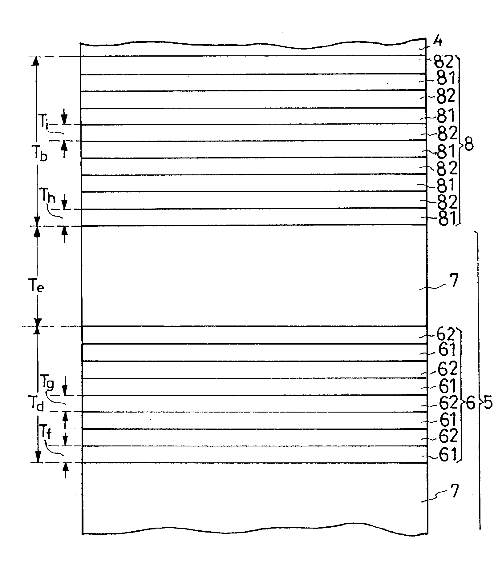
[0123]This modified semiconductor wafer 1a is similar in construction to its FIG. 2 counterpart 1 except for a first multilayered buffer subregion 5a of a buffer region 3a. The first buffer subregion 5a of the wafer 1a differs then from the first buffer subregion 5 of the buffer region 3 of the wafer 1 in the absence of that one of the non-sublayered second buffer layers 7 of the first buffer subregion 5 which forms the topmost layer of the first buffer subregion 5 in the wafer 1. Consequently, in this modified wafer 1a, the second buffer layers 7 of the first buffer subregion 5a are one less in number than those of the first buffer subregion 5 of the wafer 1. The topmost one of the multi-sublayered first buffer layers 6 of the first buffer subregion 5a forms the topmost layer of that entire subregion 5a and is joined directly to the overlying second multilayered subregion 8 of the buffer region 3a.

[0124]In this wafer 1a, too, the second multilayered buffer subregion 8 is l...


PUM


Abstract

A main semiconductor region of semiconducting nitrides is formed on a silicon substrate via a buffer region of semiconducting nitrides to provide devices such as HEMTs, MESFETs and LEDs. In order to render the wafer proof against warping, the buffer region is divided into a first and a second multilayered buffer subregion. The first buffer subregion comprises multiple alterations of a multi-sublayered first buffer layer and a non-sublayered second buffer layer. Each multi-sublayered first buffer layer of the first buffer subregion comprises multiple alternations of a first and a second buffer sublayer. The second buffer sublayers of each multi-sublayered first buffer layer either do not contain aluminum or do contain it in a higher proportion than do the first buffer sublayers. The second multilayered buffer subregion comprises multiple alternations of a first and a second buffer layer. The first buffer layers of the second multilayered buffer subregion are less in aluminum proportion than the fourth buffer layers of the second multilayered buffer subregion.

Description

CROSS REFERENCE TO RELATED APPLICATIONS[0001]This application claims priority to Japanese Patent Application No. 2007-049792, filed Feb. 28, 2007.BACKGROUND OF THE INVENTION[0002]This invention relates to semiconductor wafers, and particularly to those having nitride semiconductors grown by epitaxy on a substrate of silicon, silicon compounds or the like. The invention also specifically pertains to semiconductor devices manufacturable from the wafers, such for example as high-electron-mobility transistors (HEMTs), metal semiconductor field-effect transistors (MESFETs), and light-emitting diodes (LEDs), and to a method of making such wafers.[0003]The semiconductor wafer having layers of nitride semiconductors grown on a silicon substrate by epitaxy has been known, as disclosed for example in Japanese Unexamined Patent Publication No. 2003-59948. Silicon is preferred as a less expensive substitute for sapphire as a substrate material. However, a problem has been encountered in use of ...

Claims


Application Information

Patent Timeline
Patent Type & Authority Applications(United States)
IPC IPC(8): H01L29/15H01L21/20
CPCH01L21/02381H01L21/02458H01L21/02505H01L33/12H01L21/0254H01L29/155H01L29/2003H01L21/02507
Inventor YANAGIHARA, MASATAKA
Owner SANKEN ELECTRIC CO LTD
Why Eureka
Try Eureka