High current semiconductor power device soic package

a technology of high-current semiconductor and soic package, which is applied in the direction of semiconductor devices, semiconductor/solid-state device details, electrical apparatus, etc., can solve the problems of poor thermal performance further limitation of the use of conventional soic package in many applications, and lower assembly yield

Active Publication Date: 2008-08-28
ALPHA & OMEGA SEMICON INC
View PDF28 Cites 16 Cited by
  • Summary
  • Abstract
  • Description
  • Claims
  • Application Information

AI Technical Summary

Benefits of technology

[0007]The present invention solves the aforementioned problems by providing a high current semiconductor power device SOIC package. The novel SOIC package can be used in high current applications and used to replace TO 252 devices in many applications.

Problems solved by technology

In high current applications, conventional SOIC packages suffer from poor thermal performance due to lead frame thickness and package bottom encapsulation.
Furthermore, semiconductor dies are conventionally attached to SOIC package lead frames using thermally poor materials such as Ag epoxy.
The use of conventional SOIC packages in many applications is further limited as the SOIC package footprint does not match the TO 252 (DPAK) land pattern on printed circuit boards.
Additionally, conventional SOIC packages have an easily deformable lead frame resulting in lower assembly yield and relatively small wire bonding areas which limit the number of bonding wires that can be used to thereby reduce package electrical resistance.

Method used


Image

  • High current semiconductor power device soic package
  • High current semiconductor power device soic package
  • High current semiconductor power device soic package

Examples


Embodiment Construction

[0018]The following detailed description is of the best modes of carrying out the invention. The description is not to be taken in a limiting sense, but is made merely for the purpose of illustrating the general principles of the invention, since the scope of the invention is best defined by the appended claims.

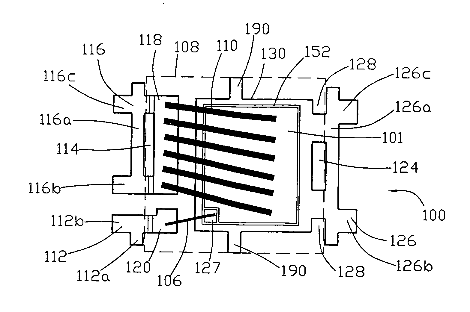
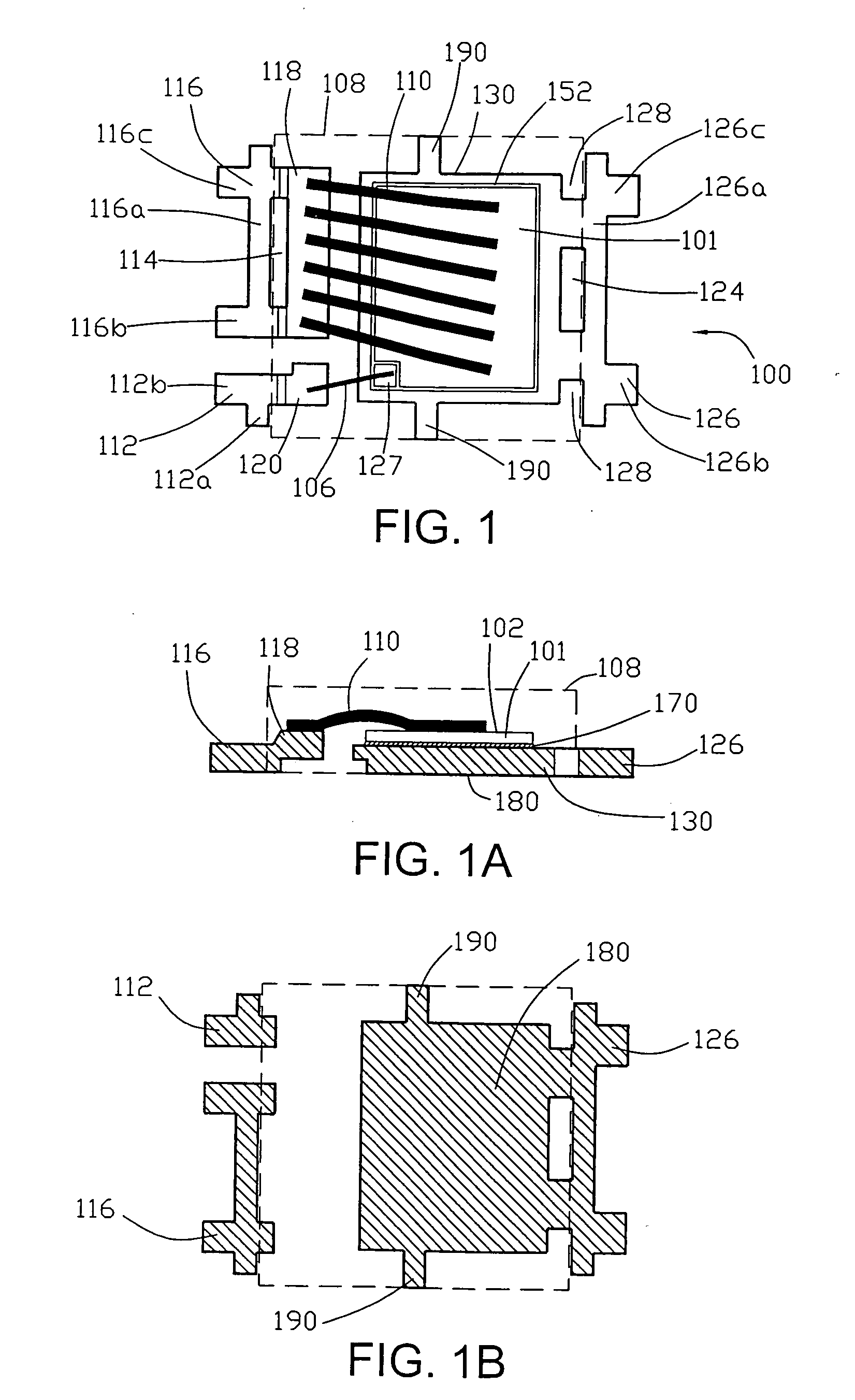
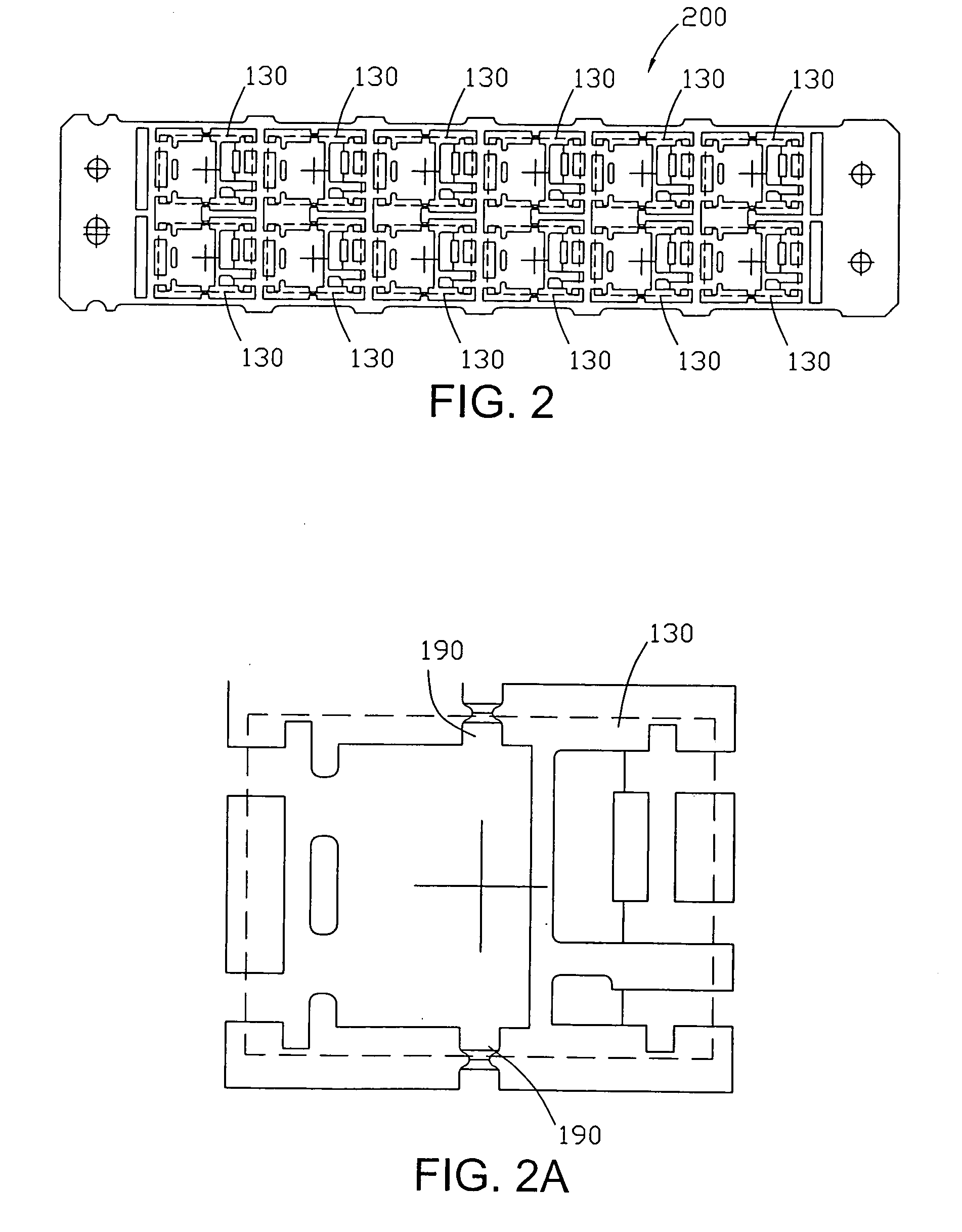
[0019]The present invention generally provides a high current semiconductor power device SOIC package having a lead frame formed of a single gauge material having a thickness greater than the conventional 8 to 10 mils. Advantageously, a thicker lead frame facilitates the bonding of larger diameter aluminum bonding wires. The use of aluminum bonding wires decreases package resistance dramatically over conventional gold wire configurations. Bonding wires may be up to 20 mils in diameter. A thicker lead frame material further provides for improved package thermal behavior by facilitating heat flow laterally out a drain lead. This is so even in a case where a bottom portion of th...


PUM


Abstract

A high current semiconductor power SOIC package is disclosed. The package includes a relatively thick lead frame formed of a single gauge material having a thickness greater than 8 mils, the lead frame having a plurality of leads and a first lead frame pad, the first lead frame pad including a die soldered thereto; a pair of lead bonding areas being disposed in a same plane of a top surface of the die; large diameter bonding wires connecting the die to the plurality of leads, the bonding wires being aluminum; and a resin body encapsulating the die, bonding wires and at least a portion of the lead frame.

Description

CROSS REFERENCE TO RELATED APPLICATIONS[0001]The present invention is a continuation in part application of Ser. No. 10 / 896,375, filed on Jul. 20, 2004 and entitled “Power Semiconductor Package”, the disclosure of which is incorporated herein by reference in its entirety.BACKGROUND OF THE INVENTION[0002]The present invention generally relates to semiconductor devices, more particularly to a high current semiconductor device SOIC package.[0003]Power semiconductor packages have evolved from through hole to surface mounted packages with the evolution of printed circuit board technology. Surface mounted packages generally include a lead frame on which a semiconductor device is mounted. The semiconductor device and a portion of the lead frame are generally encapsulated with a resin material. In a leaded package, lead terminals extend outside the resin body and include bonding pads for providing a wire bond connection from the semiconductor device to the lead terminal.[0004]Major consider...

Claims


Application Information

Patent Timeline
Patent Type & Authority Applications(United States)
IPC IPC(8): H01L23/495
CPCH01L23/492H01L23/4952H01L2924/30107H01L2924/2076H01L2924/14H01L2924/014H01L23/49562H01L24/29H01L24/45H01L24/48H01L24/49H01L24/83H01L24/97H01L2224/32245H01L2224/45015H01L2224/45124H01L2224/45144H01L2224/48091H01L2224/48247H01L2224/48472H01L2224/48599H01L2224/48699H01L2224/4903H01L2224/49051H01L2224/49111H01L2224/4943H01L2224/73265H01L2224/83801H01L2224/97H01L2924/01013H01L2924/01047H01L2924/01079H01L2924/01082H01L2924/00014H01L2224/83H01L2224/85H01L2924/00012H01L2924/00H01L24/73H01L2924/181H01L2224/0603H01L2224/85399H01L2224/05599
Inventor SUN, MINGZHANG, XIAOTIANSHI, LEI
Owner ALPHA & OMEGA SEMICON INC
Why Eureka
Try Eureka