Display substrate, method for manufacturing the same, and display apparatus having the same

a technology of display substrate and substrate, which is applied in the direction of static indicating devices, instruments, non-linear optics, etc., can solve the problems of electrostatic discharge that may damage the display apparatus, static electricity to discharge on the display apparatus, and defects due to electrostatic discharge in the display substrate, so as to prevent short circuit between the pads, reduce the effect of corrosion of the data line and efficient dissipation

Inactive Publication Date: 2008-08-28
SAMSUNG ELECTRONICS CO LTD
View PDF0 Cites 74 Cited by
  • Summary
  • Abstract
  • Description
  • Claims
  • Application Information

AI Technical Summary

Benefits of technology

[0015]According to an exemplary embodiment of the present invention, the connecting line electrically connecting the guard ring with the pad is formed before forming the second insulating layer, so that the frequency and/or severity of patterning defects of the connecting line caused at a stepped portion of the second insulating layer may be reduced or prevented. Thus, short circuits between the pads may be prevented, and static electricity that flows f

Problems solved by technology

The rubbing process may cause static electricity to discharge on the display apparatus.
For example, rubbing a negatively charged cloth against a positively charged display substrate may cause electrostatic discharge that may damage the display apparatus.
Accordingly, defects due to electrostatic discharge

Method used


Image

  • Display substrate, method for manufacturing the same, and display apparatus having the same
  • Display substrate, method for manufacturing the same, and display apparatus having the same
  • Display substrate, method for manufacturing the same, and display apparatus having the same

Examples


Embodiment Construction

[0032]Exemplary embodiments of the present invention are described more fully hereinafter with reference to the accompanying drawings. This invention may, however, be embodied in many different forms and should not be construed as limited to the embodiments set forth herein. In the drawings, the size and relative sizes of layers and regions may be exaggerated for clarity.

[0033]It will be understood that when an element or layer is referred to as being “on,”“connected to” or “coupled to” another element or layer, it can be directly on, connected or coupled to the other element or layer or intervening elements or layers may be present.

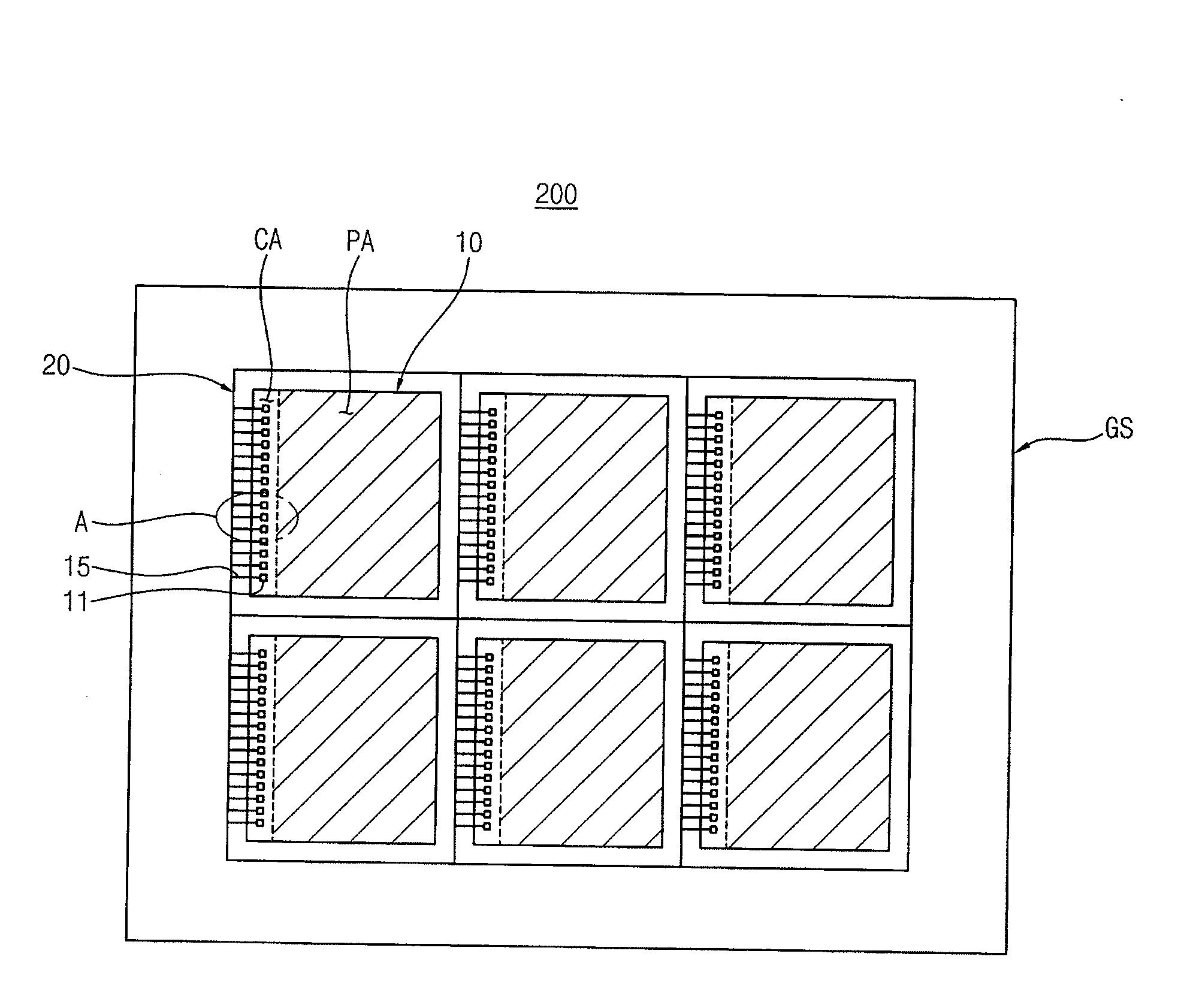
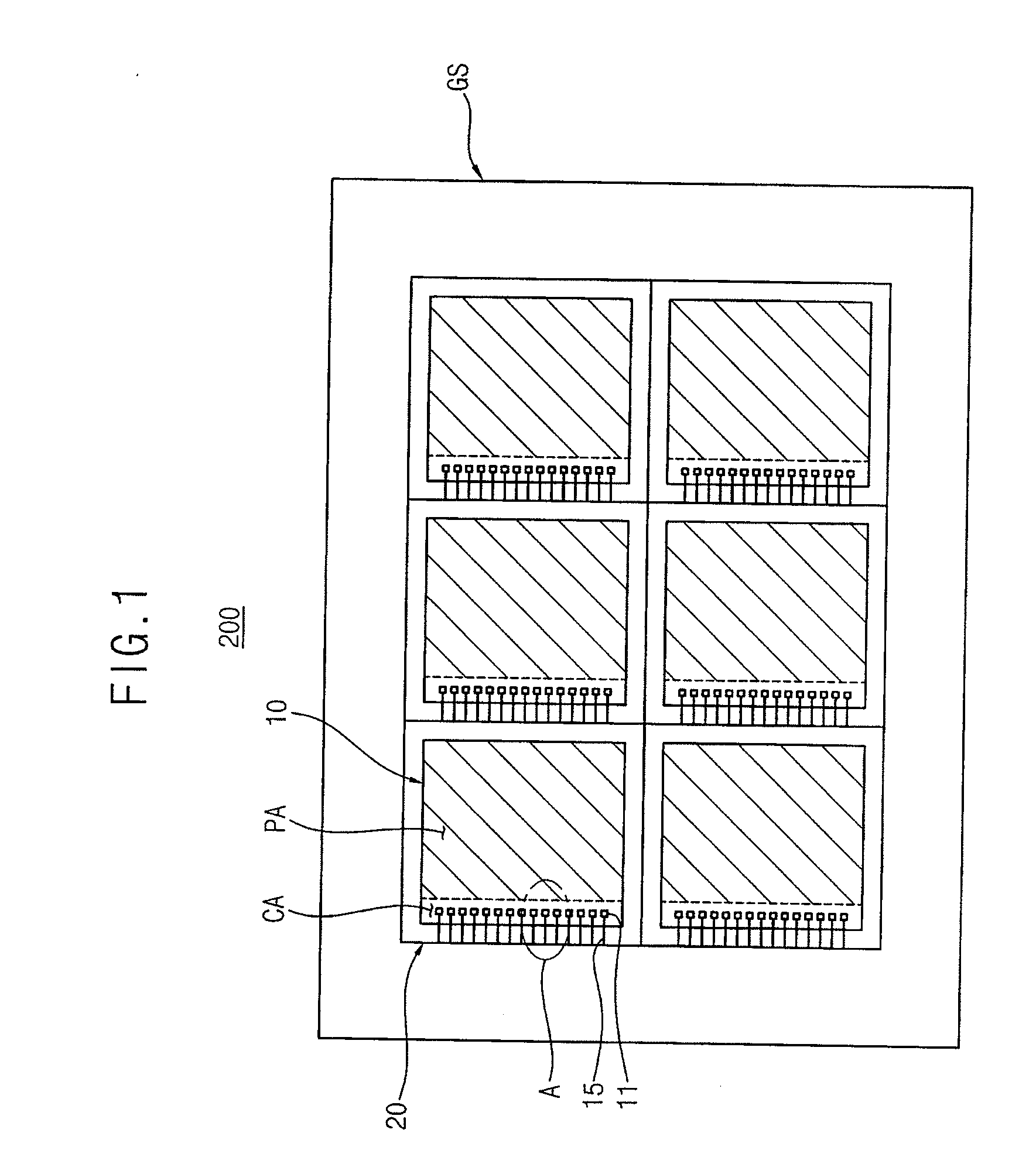
[0034]FIG. 1 is a plan view illustrating a display substrate 200 according to an exemplary embodiment of the present invention.

[0035]Referring to FIG. 1, the display substrate 200 includes a base substrate GS. An active area 10 is defined in the base substrate GS.

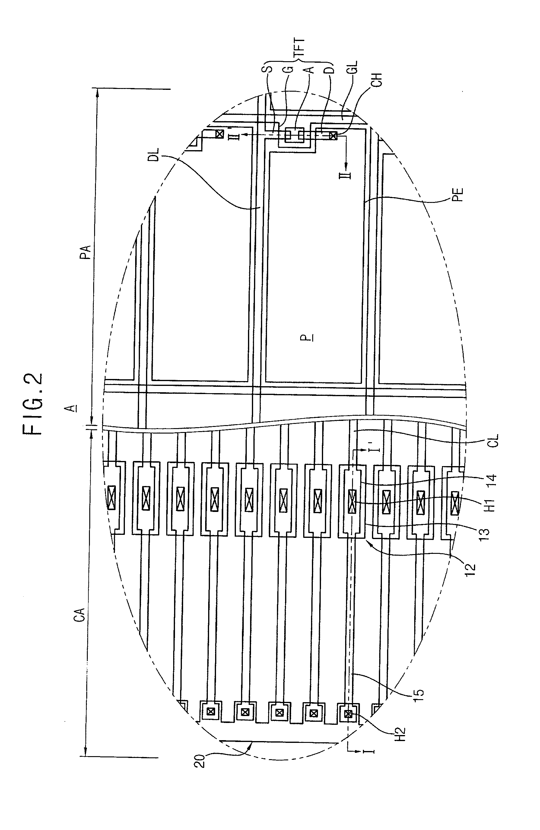
[0036]The active area 10 includes a pixel area PA and a peripheral area CA. Unit pixels incl...


PUM


Abstract

A display substrate includes a substrate, a guard ring and a connecting line. The substrate includes a plurality of active areas, and each of the active areas has a pixel area and a peripheral area. The guard ring is formed on the substrate to enclose each of the active areas, and is formed from substantially the same layer as a pixel electrode that is formed in a unit pixel. The connecting line is formed from a different layer than the guard ring, to electrically connect the guard ring with pads. The connecting line is formed before forming an organic insulating layer, and thus the frequency and/or severity of patterning defects of the connecting line may be reduced or prevented. Accordingly, short circuits between the pads may be prevented, and the corrosion resistance of the display apparatus may be increased.

Description

CROSS-REFERENCE TO RELATED APPLICATIONS[0001]This application claims priority under 35 U.S.C. §119 to Korean Patent Applications No. 10-2007-0017643, filed on Feb. 22, 2007, and No. 10-2007-0049539, filed on May 22, 2007, the contents of which are herein incorporated by reference in their entireties.BACKGROUND OF THE INVENTION[0002]1. Technical Field[0003]The present invention relates to a display substrate. More particularly, the present invention relates to a display substrate, a method for manufacturing the same and a display apparatus having the same.[0004]2. Discussion of the Related Art[0005]Methods for manufacturing a display substrate of a liquid crystal display (LCD) panel may include a rubbing process for forming textures extending along a predetermined direction on an alignment film. The rubbing process may cause static electricity to discharge on the display apparatus. For example, rubbing a negatively charged cloth against a positively charged display substrate may caus...

Claims


Application Information

Patent Timeline
IPC IPC(8): G02F1/1343G02F1/133
CPCG02F1/133351G02F2202/22G02F1/13452
Inventor JUNG, MIN-KYUNGPARK, YONG-HANNA, HYUNG-DONKIM, HYUN-YOUNG
Owner SAMSUNG ELECTRONICS CO LTD
Why Eureka
Try Eureka