Electro-static discharge protection device, semiconductor device, and method for manufacturing electro-static discharge protection device

a protection device and electrostatic discharge technology, applied in the field of semiconductor devices, including electrostatic discharge protection devices, can solve problems such as esd damage to the internal circui

Active Publication Date: 2008-09-04
SOCIONEXT INC
View PDF22 Cites 119 Cited by
  • Summary
  • Abstract
  • Description
  • Claims
  • Application Information

AI Technical Summary

Benefits of technology

[0013]One aspect of the present disclosure is an electro-static discharge protection device including a substrate and a gate electrode formed on the substrate. A first diffusion region of a first conductivity type and a second diffusion region of the first conductivity type are formed in the substrate with the gate electrode located in between. A first silicide layer is formed at a local region in a surface of the first diffusion region. The first silicide layer is electrically coupled to an electrode pad to which signal voltage is applied. A silicide block region is formed between the gate electrode and the first silicide layer. A third diffusion region is formed below the first silicide layer to partially overlap a lower end of the first diffusion region. The third diffusion region and the first silicide layer have substantially the same shapes and dimensions in a lateral direction. The third diffusion region and a portion below the gate electrode located at the same depth as the third diffusion region contain impurities of a second conductivity type that differs from the first conductivity type. The third diffusion region has an impurity concentration controlled to be higher than that of the portion below the gate electrode located at the same depth.

Problems solved by technology

This may result in the ESD damaging the internal circuit 120 before the ESD-protection-driver circuit 130 operates.

Method used


Image

  • Electro-static discharge protection device, semiconductor device, and method for manufacturing electro-static discharge protection device
  • Electro-static discharge protection device, semiconductor device, and method for manufacturing electro-static discharge protection device
  • Electro-static discharge protection device, semiconductor device, and method for manufacturing electro-static discharge protection device

Examples


second embodiment

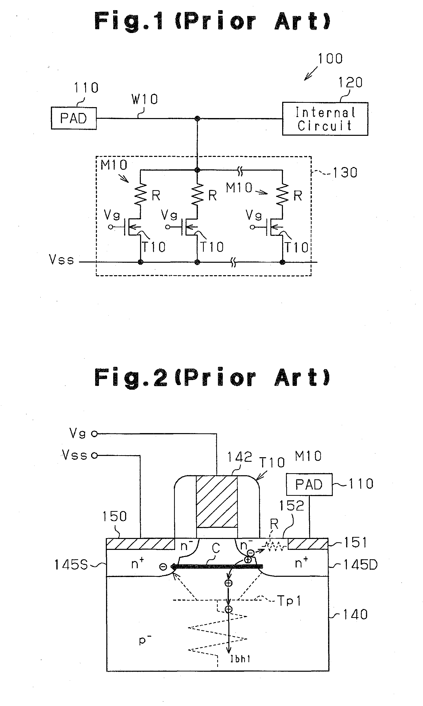
[0049]FIG. 8 shows a method for manufacturing a semiconductor device including an ESD-protection-driver circuit 60 according to the present invention. To avoid redundancy, like or same reference numerals are given to those components that are the same as the corresponding components shown in FIGS. 4 to 7. Such components will not be described in detail.

[0050]As shown in FIG. 8(a), gate electrodes 42 are formed on the surface of a substrate 40 by way of gate oxidation films 41. N-type diffusion regions 61S and 61D are respectively formed in a source formation region S and a drain formation region D by injecting phosphate ions (P+) with an energy of 30 keV while controlling the dose amount to be 3×1013 cm−2 using the gate electrodes 42 as masks.

[0051]Subsequently, as shown in FIG. 8(b), CVD is performed to apply an insulation film 62, which is formed by a silicon oxidation film, on the entire surface of the substrate 40. A photoresist P3 is formed on the insulation film 62, and the in...

third embodiment

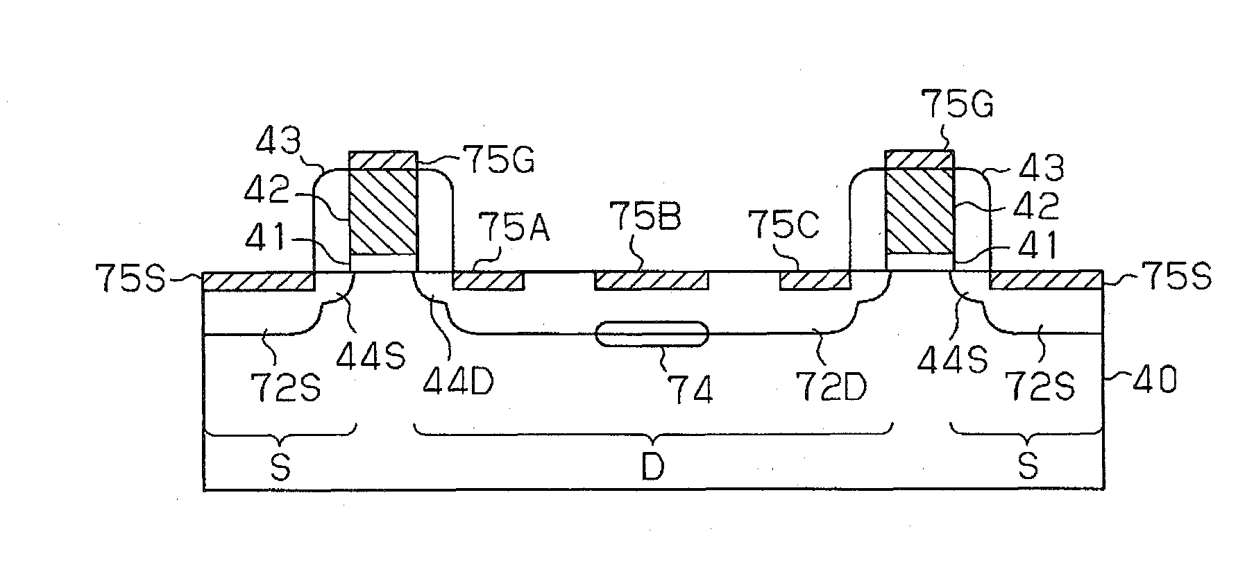
[0058]FIG. 9 shows a method for manufacturing a semiconductor device including an ESD-protection-driver circuit 70 according to the present invention. To avoid redundancy, like or same reference numerals are given to those components that are the same as the corresponding components shown in FIGS. 4 to 8. Such components will not be described in detail.

[0059]Referring to FIG. 9(a), gate electrodes 42 are formed on the surface of a substrate 40 by way of gate oxidation films 41. Further, LDD regions 44S and 44D are respectively formed in a source formation region S and drain formation region D using the gate electrodes 42 as masks. Sidewalls 43 are then formed on the gate electrodes 42.

[0060]Referring to FIG. 9(b), after performing photolithography to form a film of photoresist over the entire surface, the photoresist is patterned to a predetermined shape to form two photoresists P4 and P5 on the surface of the drain formation region D. The photoresists P4 and P5 are spaced apart fro...

first embodiment

[0065](2) The patterns of the photoresist P6 and the oxidation films P7 and P8 are set so that the p+ diffusion region 74 is formed only immediately below the silicide layer 75B serving as the drain electrode as wide as possible immediately below the silicide layer 75B. That is, the patterns of the photoresist P6 and the oxidation films P7 and P8 are set to form the p+ diffusion region 74 with substantially the same shape and dimensions in the lateral direction as the silicide layer 75B immediately below the silicide layer 75B. This obtains the same advantages as the
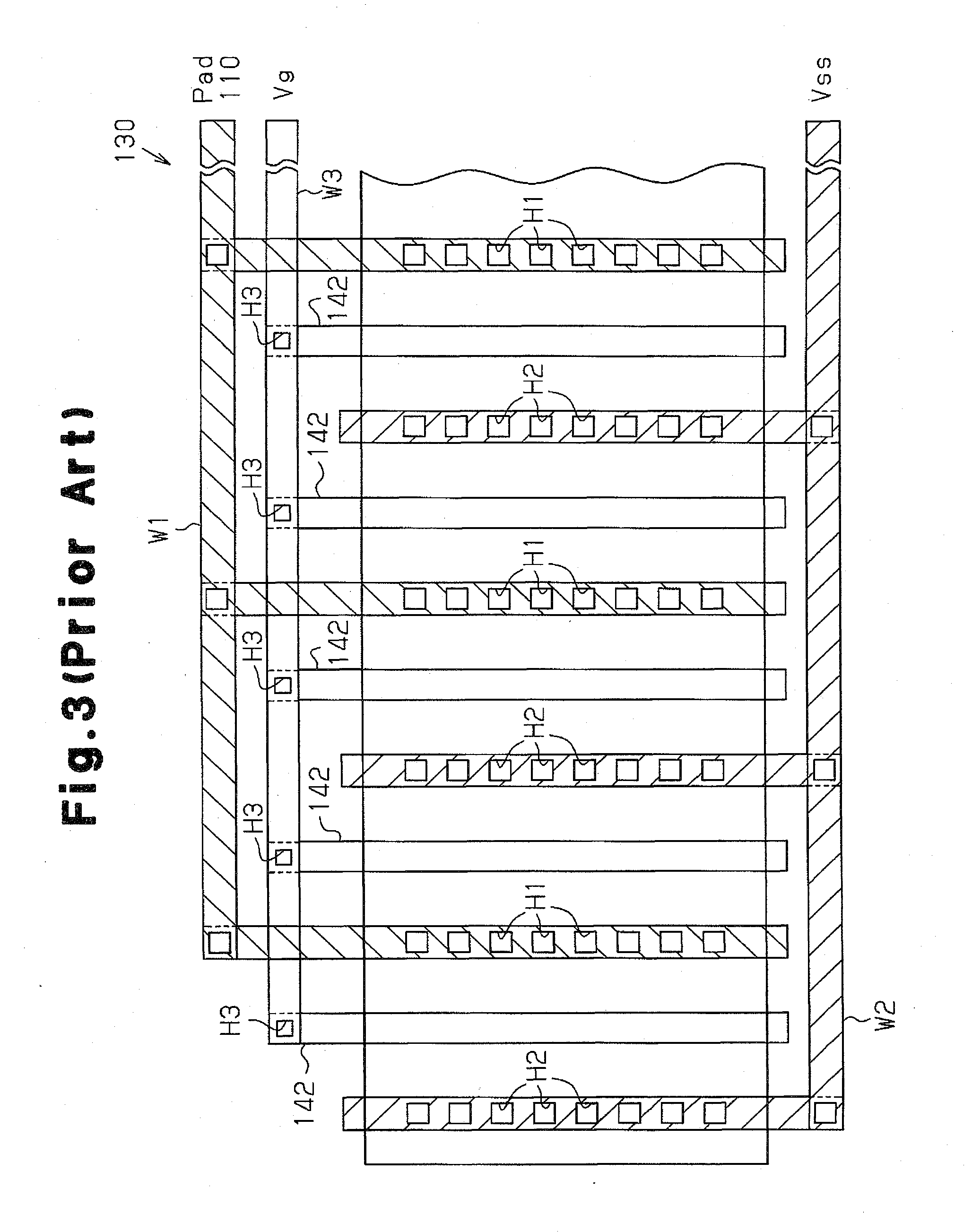

PUM


Abstract

An electrostatic discharge protection device including a gate electrode formed on a substrate. First and second diffusion regions of a first conductivity type are formed in the substrate with the gate electrode located in between. A first silicide layer is formed in the first diffusion region. A silicide block region is formed between the gate electrode and the first suicide layer. A third diffusion region is formed below the first silicide layer to partially overlap the first diffusion region. The third diffusion region and first silicide layer have substantially the same shapes and dimensions. The third diffusion region and a portion below the gate electrode located at the same depth as the third diffusion region contain impurities of a second conductivity type. The third diffusion region has an impurity concentration that is higher than that of the portion below the gate electrode.

Description

CROSS-REFERENCE TO RELATED APPLICATIONS[0001]This application is based upon and claims the benefit of priority from the prior Japanese Patent Application No. 2007-039703, filed on Feb. 20, 2007, the entire contents of which are incorporated herein by reference.BACKGROUND OF THE INVENTION[0002]1. Field[0003]The present disclosure relates to a semiconductor device, and more specifically, to a semiconductor device including an electro-static discharge protection device.[0004]2. Description of the Related Art[0005]A typical semiconductor device includes an electro-static discharge (ESD) protection circuit to protect semiconductor elements from an external ESD surge. The formation of a p+ diffusion region in a drain region at a deep portion of a substrate is known as a method for enhancing ESD robustness of an electro-static discharge element in an ESD protection circuit. In this known example, however, the AC characteristics vary during normal operation of an IO cell depending on the ac...

Claims


Application Information

Patent Timeline
Patent Type & Authority Applications(United States)
IPC IPC(8): H01L27/06H01L21/336
CPCH01L21/823425H01L27/0266H01L21/04H01L29/7833H01L29/1087H01L23/60H01L27/04
Inventor SUZUKI, TERUO
Owner SOCIONEXT INC
Why Eureka
Try Eureka