Light Emitting Diode and Method of Fabricating the Same

Active Publication Date: 2008-09-11
SEOUL SEMICONDUCTOR
View PDF15 Cites 20 Cited by
  • Summary
  • Abstract
  • Description
  • Claims
  • Application Information

AI Technical Summary

Benefits of technology

[0010]The present invention is conceived to solve the aforementioned problems in the prior arts. Accordingly, an object of the present invention is to provide a light emitting diode and a method of fabricating the same, wherein the distance between a fluorescent substance and a light emitting diode chip is uniformly maintained when the fluorescent substance is applied to the light emitting diode, thereby reducing a color variation, i.e., generation of two or more different colors, and enhancing luminous efficiency.

Problems solved by technology

A difference in concentration within the liquid epoxy resin occurs due to such precipitation of the fluorescent substance, and thus, there is a problem with color reproducibility because light emitted from the light emitting diode chip is not uniform.
Further, since a color speckle is produced, a great amount of fluorescent substance should be contained in the molding portion to express a uniform color, resulting in degradation of light emitting efficiency.
Furthermore, since the fluorescent substance is not uniformly distributed, there is a problem in that the color of light emitted from the light emitting diode varies depending on an angle at which the light emitting diode is viewed.
Thus, there is a problem in that the distance between the light emitting diode and the fluorescent substance varies and thus a color may not be uniformly expressed and two or more different colors may be produced depending on a light emitting region.
Further, in case of FIG. 4, the luminous efficiency of light considerably decreases due to interference between the light emitting diode chip and the reflecting portion.
However, since an additional process should be added to attach the guide member 90, a fabricating process becomes complicated, resulting in increased production costs.
Further, there is a problem in that luminous efficiency decreases and a great amount of fluorescent substance is consumed due to the guide member.

Method used


Image

  • Light Emitting Diode and Method of Fabricating the Same
  • Light Emitting Diode and Method of Fabricating the Same
  • Light Emitting Diode and Method of Fabricating the Same

Examples


first embodiment

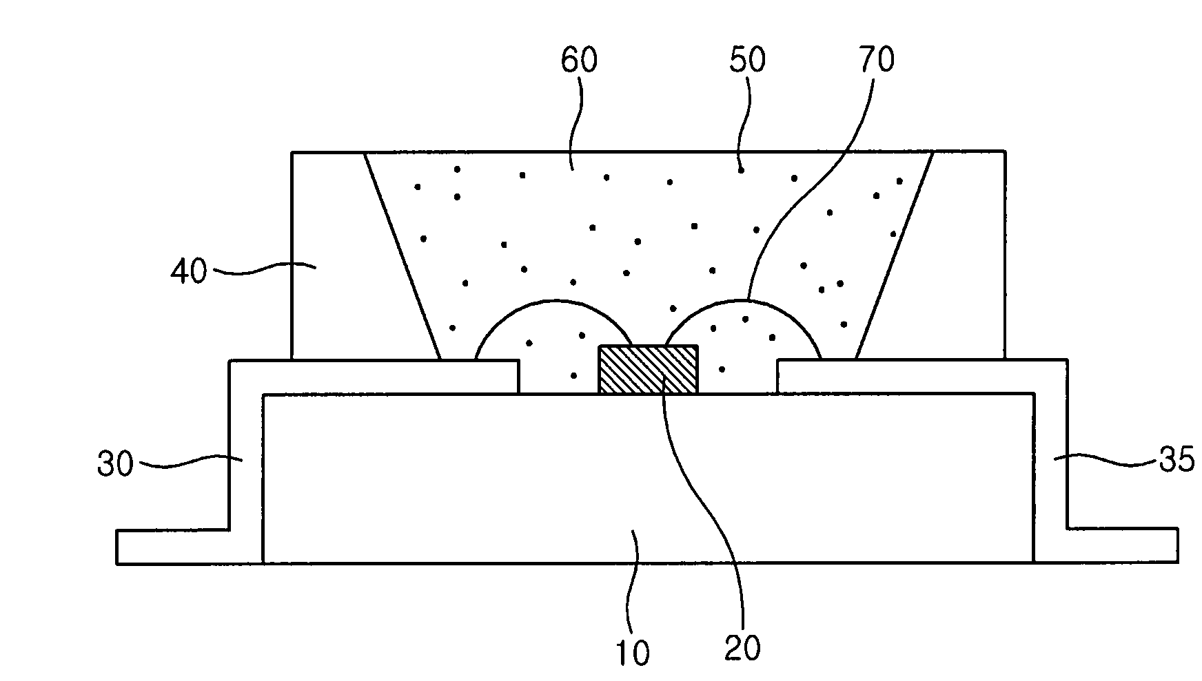
[0037]FIGS. 6 and 7 are a perspective view and a sectional view of a light emitting diode according to the present invention, respectively. That is, the figures are a perspective view and a sectional view of a chip-type light emitting diode according to the present invention, respectively.

[0038]Referring to FIGS. 6 and 7, the light emitting diode comprises a substrate 210 with lead terminals 230 and 235 formed thereon, a frame 290 formed on the substrate 210, a light emitting diode chip 220 mounted on the frame 290, and wires 270 for connecting the light emitting diode chip 220 to the lead terminals 230 and 235. Further, a fluorescent substance 250 for converting the wavelength of light generated from the light emitting diode chip 220 is mixed with an encapsulant and then applied to the frame 290 to form a molding portion 260. Although the light emitting diode of this embodiment includes one light emitting diode chip 220, it is only for illustrative purposes and the light emitting d...

second embodiment

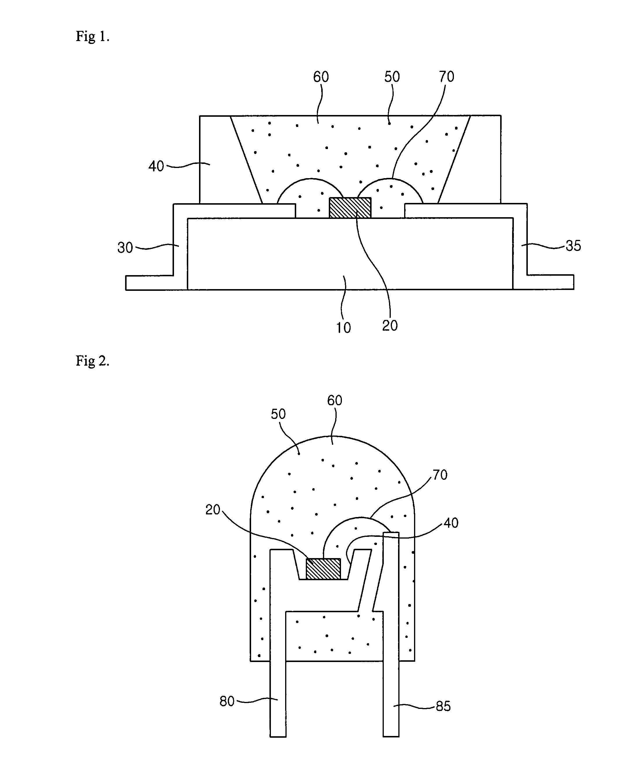
[0042]FIG. 8 is a sectional view of a light emitting diode according to the present invention, namely. That is, the figure is a schematic sectional view of a top-type light emitting diode according to the present invention.

[0043]Referring to FIG. 8, the light emitting diode of the second embodiment is similar to that of the first embodiment except that a reflecting portion is formed on a substrate. Thus, only parts different from each other will be described below.

[0044]The light emitting diode comprises a substrate 210, lead terminals 230 and 235 formed on the substrate, a frame 290, a reflecting portion 240, a light emitting diode chip 220 mounted on the frame 290, and wires 270 for connecting the light emitting diode chip 220 to the lead terminals 230 and 235. Further, a fluorescent substance 250 for converting the wavelength of light generated from the light emitting diode chip 220 is mixed with an encapsulant and then applied to the frame 290 to form a molding portion 260. A pe...

third embodiment

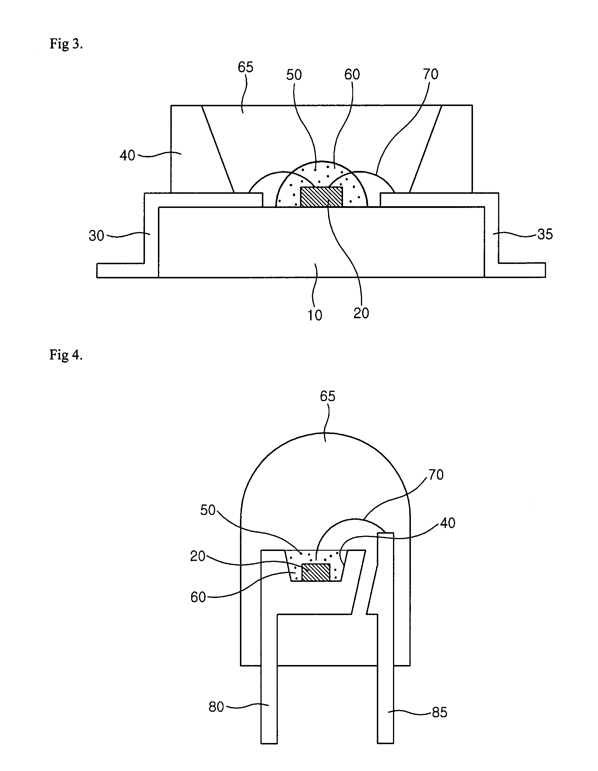
[0046]FIG. 9 is a sectional view of a light emitting diode according to the present invention. That is, this figure is a schematic sectional view of a lamp-type light emitting diode according to the present invention.

[0047]Referring to FIG. 9, the light emitting diode comprises a first lead terminal 330 with a reflecting portion 340 at a top end thereof, and a second lead terminal 335 spaced apart by a predetermined distance from the first lead terminal 330. Further, a frame 390 is formed inside the reflecting portion 340 of the first lead terminal 330, and a light emitting diode chip 320 is mounted on the frame 390.

[0048]Furthermore, a fluorescent substance 350 for converting the wavelength of light generated from the light emitting diode chip 320 is mixed with an encapsulant and then applied to the frame 390 to form a molding portion 360. A peripheral molding portion 365 is formed on the light emitting diode chip 320 by applying a predetermined resin thereto and thermally curing t...


PUM


Abstract

The present invention relates to a light emitting diode and a method of fabricating the same, wherein the distance between a fluorescent substance and a light emitting diode chip is uniformly maintained to enhance luminous efficiency. To this end, there is provided a light emitting diode comprising at least one light emitting diode chip, lead terminals for use in applying electric power to the light emitting diode chip, and a frame that is used for mounting the light emitting diode chip thereon and is formed to have a predetermined height and a shape corresponding to that of the light emitting diode chip.

Description

TECHNICAL FIELD[0001]The present invention relates to a light emitting diode and a method of fabricating the same, and more particularly, to a light emitting diode with a frame structure for allowing uniform application of a fluorescent substance thereon and a method of fabricating the light emitting diode.BACKGROUND ART[0002]FIGS. 1 and 2 are schematic sectional views of light emitting diodes in which a fluorescent substance is applied in accordance with a prior art. FIG. 1 is a sectional view of a conventional top-type light emitting diode and FIG. 2 is a sectional view of a conventional lamp-type light emitting diode.[0003]Referring to FIG. 1, the light emitting diode comprises a substrate 10 with first and second lead terminals 30 and 35 formed thereon, a light emitting diode chip 20 mounted on the substrate 10, and a reflecting portion 40 formed on the substrate to surround the light emitting diode chip 20. The light emitting diode chip 20 is electrically connected to the first...

Claims


Application Information

Patent Timeline
IPC IPC(8): H01L33/00H01L21/50H01L33/50H01L33/54H01L33/56H01L33/62
CPCH01L33/505H01L33/54H01L33/62H01L2224/48091H01L2224/48247H01L2224/8592H01L2933/0041H01L2224/45139H01L2924/00014H01L2924/00H01L2924/181H01L2924/00011H01L2924/00012H01L2924/01049H01L2924/01005H01L2224/45015H01L2924/207
Inventor KIM, DO HYUNGLEE, CHUNG-HOON
Owner SEOUL SEMICONDUCTOR
Why Eureka
Try Eureka