

Novel SyAF structure to fabricate Mbit MTJ MRAM
- Summary
- Abstract
- Description
- Claims
- Application Information
AI Technical Summary
Benefits of technology
Problems solved by technology
Method used
Image

Examples
Example
COMPARATIVE EXAMPLE 1
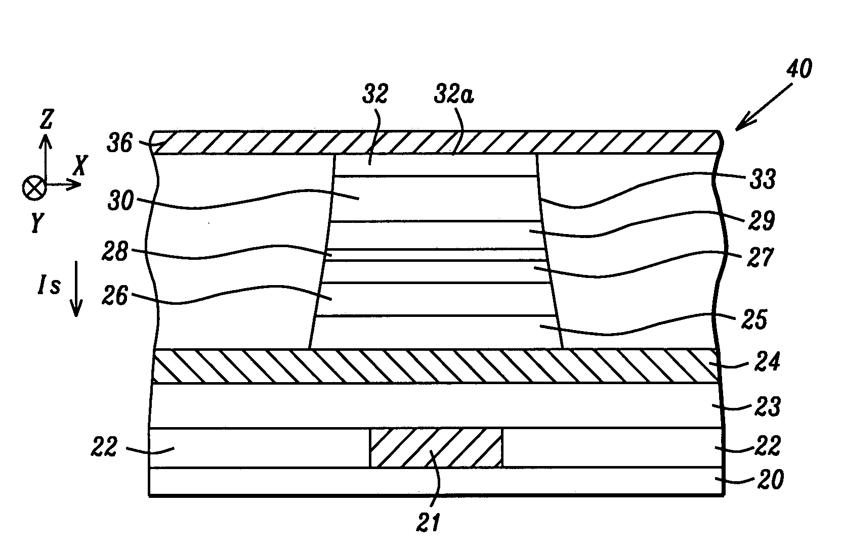
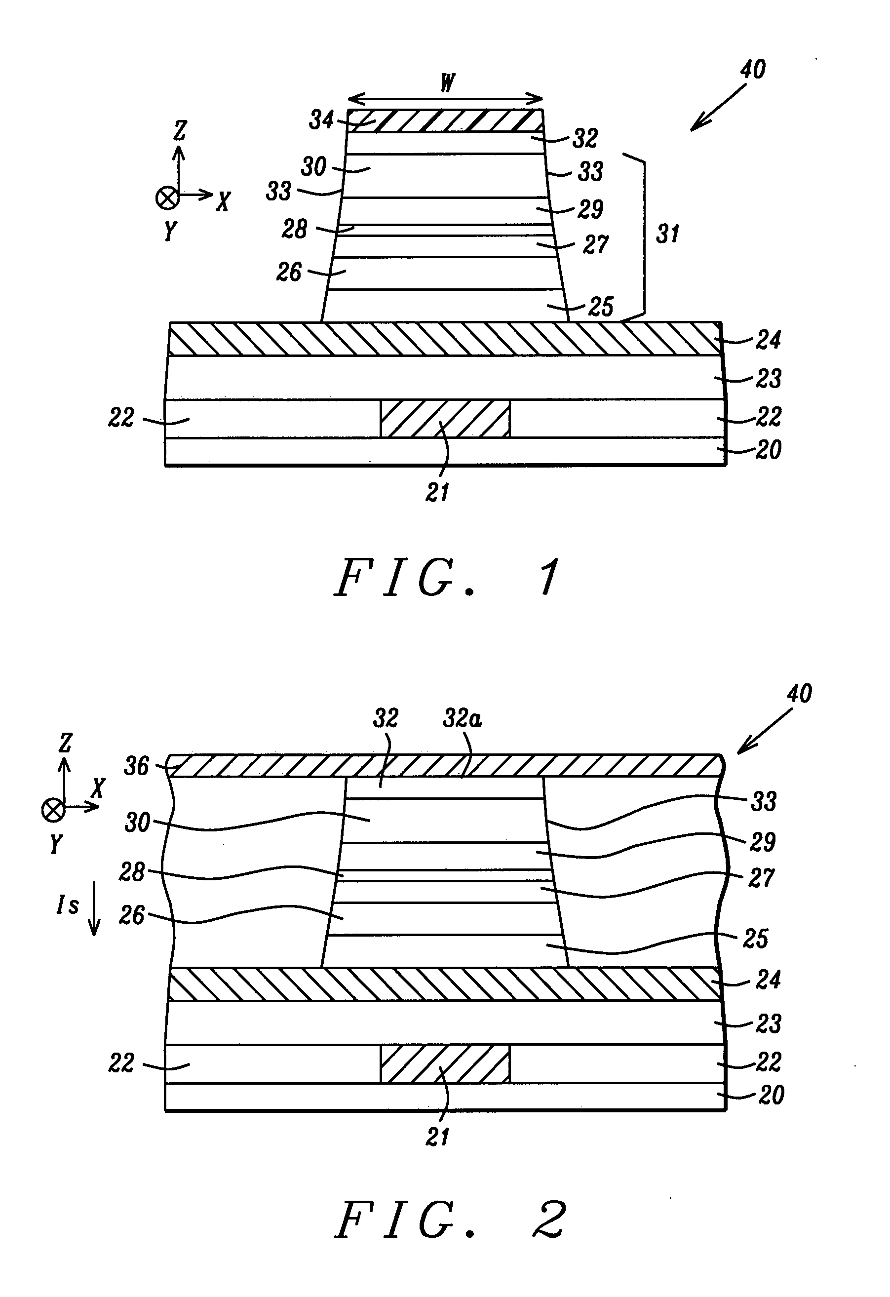
[0045]An experiment was conducted to compare the performance of a MTJ fabricated according to the present invention with a conventional MTJ based on a CoFeB / AlOx / NiFe AP1 pinned layer / tunnel barrier / free layer configuration. In this experiment, the MTJ stack is formed on a Ta / Ru200 / α-Ta100 bottom electrode and has the following succession of layers and thicknesses in order from bottom to top: 45 Angstrom NiCr seed layer; 150 Angstrom MnPt AFM layer; Co75Fe2520 / Ru7.5 / AP1 SyAF pinned layer; AlOx tunnel barrier; 29 Angstrom Ni88Fe12 free layer; and a NiFeHf45 / Ta30 / Ru100 capping layer wherein the NiFeHf configuration is represented by [(Ni88Fe12)]85Hf15. The AlOx tunnel barrier was prepared by depositing an 8.25 Angstrom thick Al layer and then oxidizing with a ROX process for 65 seconds with a O2 flow rate of 0.6 standard liters per minute and a RF power of 800 watts. Only the AP1 layer composition is varied in order to compare a Co60Fe20B20 AP1 layer from the prio...
Example
COMPARATIVE EXAMPLE 2
[0048]As mentioned previously, an AlOx tunnel barrier can be made into a “stronger oxidation” state or more highly oxidized state than normal by extending the ROX cycle time. As a result, an 8.25 Angstrom thick Al deposited layer may be transformed into an AlOx layer with a stronger oxidation state to give a higher MR and higher RA (2500 Ω-μm2 vs. 1100 Ω-μm2 POR) value. According to the present invention, an AP1 layer wherein a crystalline CoFe layer contacts the AlOx tunnel barrier provides a higher MR than an amorphous CoFeB AP1 layer since the former has a higher spin polarization. Alternatively, a higher RA MTJ can be produced by oxidizing a thicker Al film having an 8.5 to 9 Angstroms thickness, for example. The inventors have discovered that in both cases an improved quality tunnel barrier is formed with better film uniformity and less tunneling hot spots that result in a lower error count (EC) as indicated in Table 2. EC is understood to include shorts, o...
Example
COMPARATIVE EXAMPLE 3
[0051]In a third set of experiments, the error count (EC) for a plurality of samples was determined in order to assess MTJ performance for 1-Mbit MRAM applications. Table 3 is a summary of results including EC where EC(best) is the error count for the best chip in the 86 chips (across the wafer) tested while EC(mean) is the mean value for EC for the MTJ MRAM wafer. MTJs in rows 1 and 2 represent POR samples that are made with a CoFe / Ru / CoFeB SyAF pinned layer, NiFe(17.5-21%) free layer, Ru / Ta / Ru100 capping layer, and a Ta500 hard mask. The AlOx tunnel barrier is made with an A18.25 / ROX 65-70 second process to give a RA of about 950 Ω-μm2. TMR is ˜40% and V50 (bias voltage at which TMR is reduced to half is about 650 mV. In rows 1 and 2, the EC for the best chip is≧50.
TABLE 3Magnetic Properties of MTJs with BE / NiCr45 / MnPt150 / Co75Fe2520 / Ru7.5 / AP1 / AlOx(ROX) / NiFe free layer / capping layer configurationCappingRp-V50ECECRowAP1AlOxFree layerlayerRAMRRpcov(mV)bestmean1Co...
PUM
 Abstract
Description
Claims
Application Information