Method of fabricating semiconductor laser diode apparatus and semiconductor laser diode apparatus
a laser diode and semiconductor technology, applied in the direction of lasers, semiconductor lasers, solid-state devices, etc., can solve the disadvantageous problem of handling the semiconductor laser diod
- Summary
- Abstract
- Description
- Claims
- Application Information
AI Technical Summary
Problems solved by technology
Method used
Image

Examples
first embodiment
[0076]A structure of a semiconductor laser diode according to a first embodiment will be now described with reference to FIGS. 13 to 15.
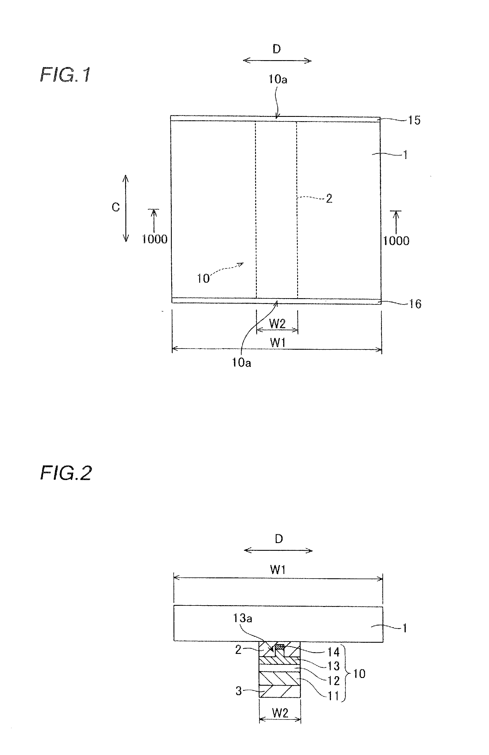
[0077]In the semiconductor laser diode according to the first embodiment, a conductive support substrate 31 made of Cu—W having no cleavability and a semiconductor laser diode portion 80 are bonded to each other through a conductive adhesive layer 44 made of AuSn, as shown in FIGS. 13 and 14. The support substrate 31 is an example of the “second substrate” and the “substrate” in the present invention, and the semiconductor laser diode portion 80 is an example of the “first semiconductor laser diode portion” in the present invention. A pair of cavity planes 90 formed by cleavage planes are formed on ends in a direction C of the semiconductor laser diode portion 80.
[0078]According to the first embodiment, a length (cavity length) L1 in the direction C of the semiconductor laser diode (support substrate 31) is about 600 μm and a width (length) W11 in a...
first modification
of First Embodiment
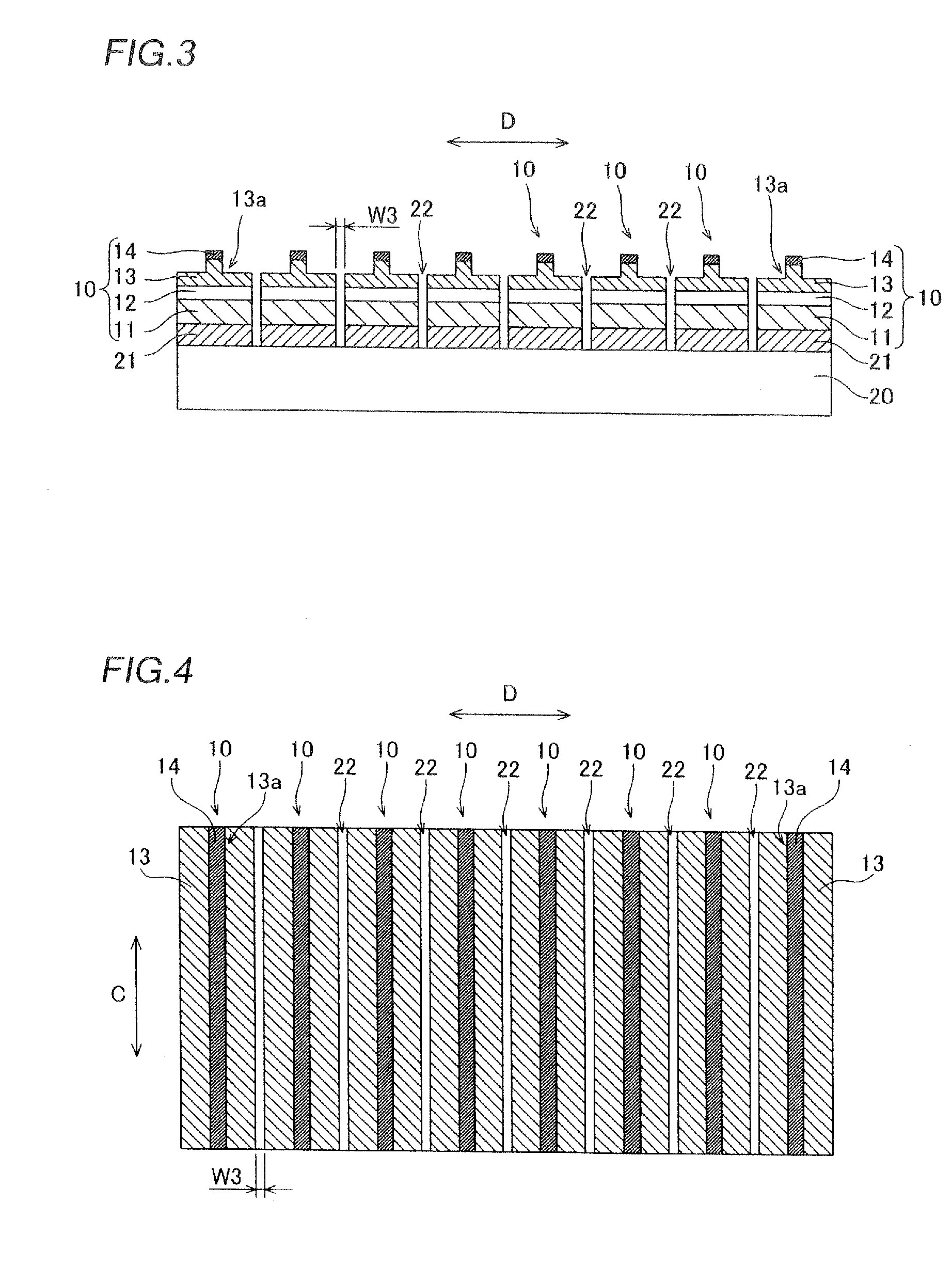
[0111]Referring to FIG. 24, a semiconductor laser diode portion 80 is bonded to a support substrate 31 formed with a projecting portion 31b in a prescribed region in a semiconductor laser diode according to a first modification of the first embodiment, dissimilarly to the aforementioned first embodiment.
[0112]In the semiconductor laser diode portion 80 according to the first modification of the first embodiment, the semiconductor laser diode portions 80 are bonded onto the projecting portions 31b previously formed on a surface of the support substrate 31 to which the semiconductor laser diode portions 80 are bonded, through adhesive layers 44, as shown in FIG. 24. Each projecting portion 31b has a height of about 5 μm and the width of each projecting portion 31b in a direction D is substantially the same as a width W13 (about 45 μm) of the p-side pad electrode 42 of the semiconductor laser diode portion 80. Therefore, outer portions 41b of insulating films 41 are ...
second modification
of First Embodiment
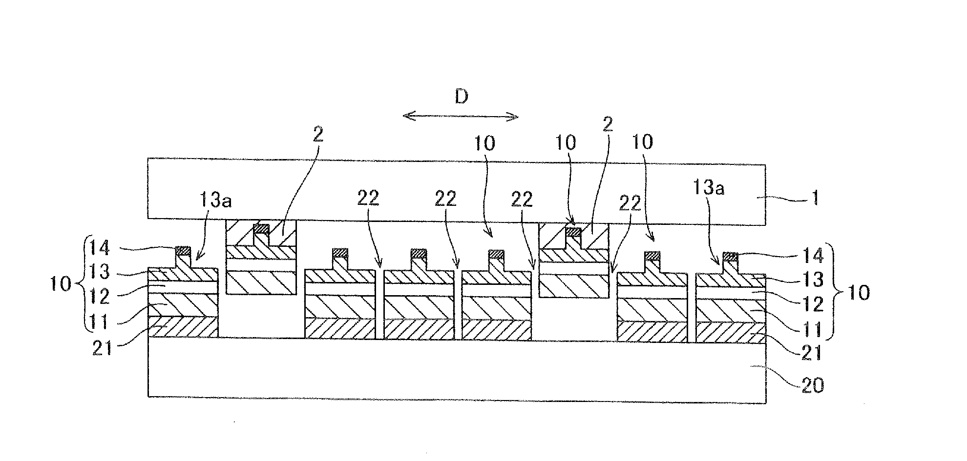
[0116]Referring to FIGS. 25 and 26, a plurality of semiconductor laser diode portions 80 are bonded to a common support substrate 31 and arrayed in a semiconductor laser diode chip according to a second modification of the first embodiment, dissimilarly to the aforementioned first embodiment.
[0117]According to the second modification of the first embodiment, a p-side electrode (support substrate 31) and an n-side electrode (n-side pad electrode 46) are employed as common electrodes respectively, and the plurality of semiconductor laser diode portions 80 each having the structure similar to that of the aforementioned first embodiment are bonded to the support substrate 31 and arrayed in a direction D, as shown in FIG. 25.
[0118]In a process of fabricating the semiconductor laser diode chip according to the second modification of the first embodiment, every two semiconductor laser diode portions 80 are bonded to the one support substrate 31 through the adhesive layer...
PUM
 Abstract
Description
Claims
Application Information
 - Generate Ideas
- Intellectual Property
- Life Sciences
- Materials
- Tech Scout
- Unparalleled Data Quality
- Higher Quality Content
- 60% Fewer Hallucinations
Browse by: Latest US Patents, China's latest patents, Technical Efficacy Thesaurus, Application Domain, Technology Topic, Popular Technical Reports.
© 2025 PatSnap. All rights reserved.Legal|Privacy policy|Modern Slavery Act Transparency Statement|Sitemap|About US| Contact US: help@patsnap.com