Semiconductor device mounted on substrate, and manufacturing method thereof

a technology of semiconductor devices and substrates, applied in the manufacture of printed circuits, printed circuit aspects, basic electric elements, etc., can solve the problems of large and small thermal load imposed on the substrate or the installed part. , to achieve the effect of cost saving

Inactive Publication Date: 2008-09-18
NEC CORP
View PDF4 Cites 32 Cited by
  • Summary
  • Abstract
  • Description
  • Claims
  • Application Information

AI Technical Summary

Benefits of technology

[0029]Further, formation of the Au stud is not necessitated. Thus, the cost is inexpensiv

Problems solved by technology

However, the soldering practice at a high temperature imposes a large thermal load upon a substrate or an installed part.
Thus, when the stress is applied, the film is prone to be exfoliated.
Thus, the thermal load imposed upon the substrate or the installed part is

Method used


Image

  • Semiconductor device mounted on substrate, and manufacturing method thereof
  • Semiconductor device mounted on substrate, and manufacturing method thereof
  • Semiconductor device mounted on substrate, and manufacturing method thereof

Examples


first embodiment

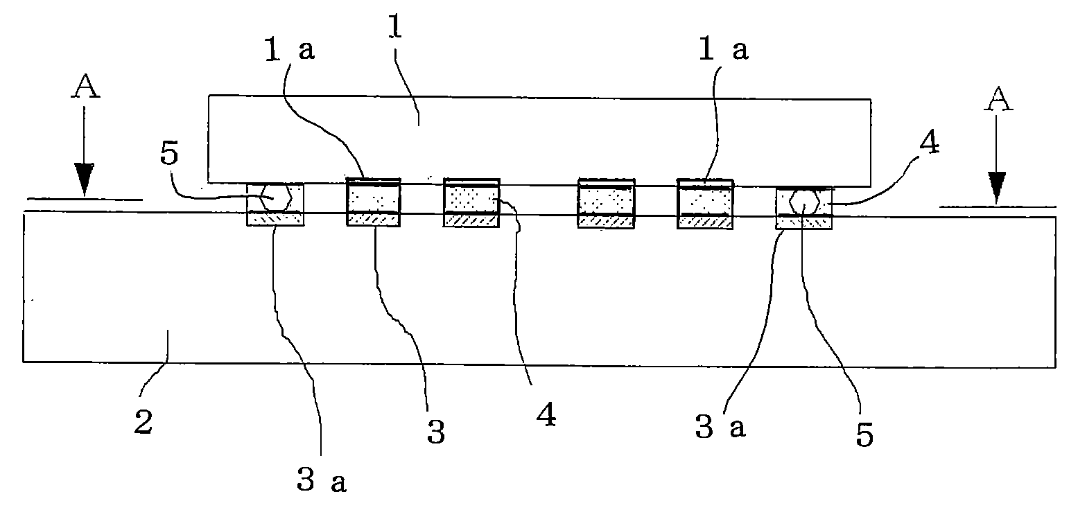
[0042]FIG. 1 shows the first embodiment of the present invention, FIG. 1a is a cross-sectional view, and FIG. 1b is a cross-sectional view in the substrate side taken across an A-A line of FIG. 1a.

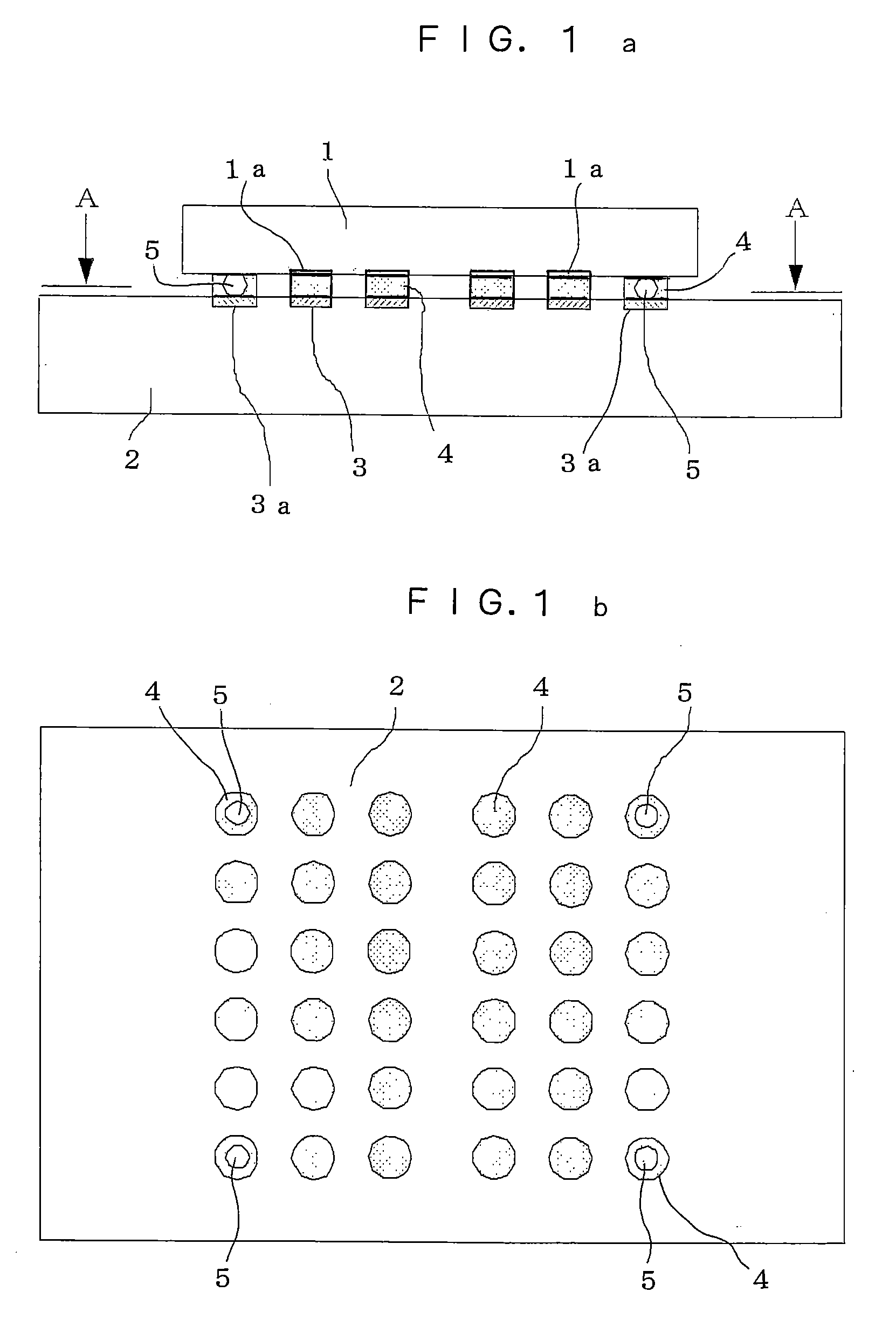
[0043]In FIG. 1a,1b, 1 is an LSI chip (semiconductor device). 1a is an electrode pad provided in the LSI chip 1.

[0044]2 is a substrate. Additionally, the parts such as a semiconductor chip such as other LSI, a resister, and a condenser may be mounted on the substrate 2. Further, the substrate 2 could be a rigid or a flexible resin substrate. Further, the substrate 2 could be a ceramic substrate. A wiring may be formed on one side or both sides of the substrate. Moreover, the wiring could be a multi-layer wiring. Further, the substrate 2 could be a BGA carrier substrate or a CSP carrier substrate.

[0045]3 is an electrode pad provided in the substrate 2. Additionally, the position of an electrode pad 1a and that of the electrode pad 3 correspond to each other. That is, in a case of mounting ...

second embodiment

[0058]FIG. 3 is a cross-sectional view illustrating the second embodiment of the present invention.

[0059]In FIG. 3, and FIG. 1a, the identical numerical code is affixed to the identical part, and the detailed explanation is omitted.

[0060]In this embodiment, the substrate 2 does not have the dummy pad 3a. Further, the spacer 5 arranged in the location that corresponds to the four corners of the LSI chip 1 is a spacer bonded with a non-conductive adhesive 6.

[0061]In the first embodiment, the arrangement position of the spacer 5 was pre-coated with the conductive adhesive. However, in this method, the quantity of the conductive adhesive with which the above location is coated is prone to be excessive. Doing so incurs the possibility that the short circuit occurs between the pads via the conductive adhesive on the dummy pad.

[0062]Thereupon, in this embodiment, the coating step with the adhesive 6 was provided apart from the coating step with the conductive adhesive 4. And, the arrangeme...

third embodiment

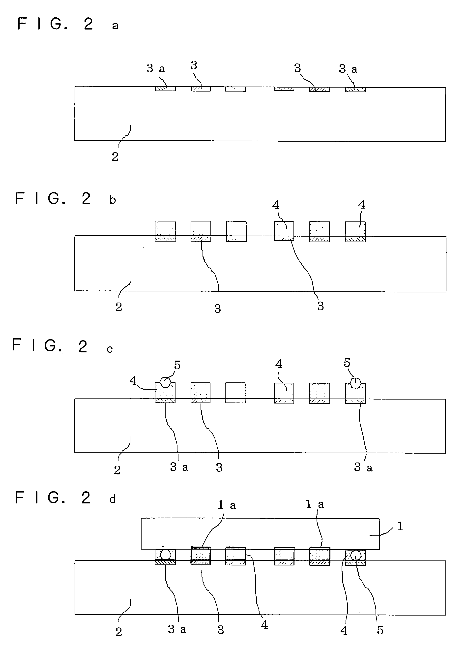
[0063]FIG. 4a,4b,4c is a view (cross-sectional view) of the step of manufacturing the device of the third embodiment of the present invention.

[0064]At first, the pad 3 of the substrate 2 similar to that of the case of the first embodiment is coated with the conductive adhesive 4 by means of the screen print method or the like (see FIG. 4a). Additionally, the dummy pad 3a is not coated with the conductive adhesive 4.

[0065]Next, the spacer 5 of which the surface has been uniformly coated with the adhesive 6 is arranged on the dummy pad 3a (see FIG. 4b).

[0066]Thereafter, the LSI chip 1 is mounted on the substrate 2 so that the electrode pad 3 of the substrate 2 coincides with the electrode pad 1a of the LSI chip 1 (see FIG. 4c).

[0067]And, the heat treatment is performed, thereby to harden the conductive adhesive 4. With this, the device of the present invention is obtained.


PUM


Abstract

The connection technology is provided in which, at the time of mounting the semiconductor device on the substrate, the thermal load or the stress, which is imposed upon the semiconductor device, is little, a reliability of the semiconductor device is obtained, a stand-off of the semiconductor device mounted on the substrate can be secured appropriately, and moreover the short circuit hardly occurs between the pads of the semiconductor device mounted on the substrate.
The semiconductor device mounted on the substrate, in which the substrate includes an electrode pad, the semiconductor device includes an electrode pad, the electrode pad of the semiconductor device and the electrode pad of the substrate are connected with a conductive adhesive, and a spacer is provided between the semiconductor device and the substrate.

Description

INCORPORATION BY REFERENCE[0001]This application is based upon and claims the benefit of priority from Japanese patent application No. 2007-059513, filed on Mar. 9, 2007, the disclosure of which is incorporated herein in its entirety by reference.RELATED ART[0002]The present invention relates to a semiconductor device mounted on a substrate. The present invention, more particularly, relates to a device in which an electrode pad of a semiconductor device such as an LSI and an electrode pad of a substrate are connected with a conductive adhesive.[0003]The semiconductor device such as the LSI is packaged on the substrate (a print substrate: a package substrate) with a flip chip bonding. For example, a solder ball or a solder bump is employed for this packaging. For example, Sn—Pb lead solder has been employed as a solder material.[0004]As it is, the lead (Pb) solder has begun to be kept at a distance due to the environmental problem. That is, the solder material that dose not contain l...

Claims


Application Information

Patent Timeline
IPC IPC(8): H01L23/48
CPCH01L23/49838H01L2924/07802H01L24/81H01L24/83H01L2224/0401H01L2224/06515H01L2224/10152H01L2224/14515H01L2224/16225H01L2224/838H01L2924/01013H01L2924/01029H01L2924/01046H01L2924/01047H01L2924/01079H01L2924/01082H01L2924/01322H01L2924/0781H01L2924/14H01L2924/19041H05K3/303H05K3/321H05K2201/09781H05K2201/10674H05K2201/2036H01L2224/2919H01L2924/01005H01L2924/01006H01L2924/01019H01L2924/01033H01L2924/0105H01L2924/014H01L2924/0665H01L24/16H01L2224/29364H01L2224/29355H01L2224/29347H01L2224/29344H01L2224/29339H01L2224/29316H01L2924/0132H01L2924/0133H01L2924/15787H01L2224/2929H01L2224/29111H01L2224/13111H01L2224/293H01L2924/00H01L2924/00014H01L2924/00015H01L2224/10165H01L2224/8114
Inventor HORI, EIJI
Owner NEC CORP
Why Eureka
Try Eureka