Organic el light emitting device and method for manufacturing the same

a light emitting device and organic el technology, applied in the direction of electric discharge tube/lamp manufacture, discharge tube luminescnet screen, semiconductor/solid-state device details, etc., can solve the problem of uneven light emission luminance (luminance gradient), insufficient light emission, and insufficient light emission to drastically lower the electrical resistivity

Inactive Publication Date: 2008-09-18
YAMAGATA PROMOTIONAL ORG FOR INDAL TECH
View PDF3 Cites 22 Cited by
  • Summary
  • Abstract
  • Description
  • Claims
  • Application Information

AI Technical Summary

Benefits of technology

[0024]The present invention has been made in view of the technical problems, and an object of the present invention is to provide an organic EL light emitting device, which has a plurality of divided light emitting segments connected in series and can be manufactured with high efficiency especially by omitting separate coating of organic EL light emitting layers with the use of a vapor-deposition mask, and a method for manufacturing the organic EL light emitting device.

Problems solved by technology

Thus, as described above, when the EL element is constituted as a surface light emitting source having a large area, unevenness in light emission luminance (luminance gradient) occurs due to the voltage drop in the transparent electrode.
Accordingly, the further from a feeding point with respect to the transparent electrode, the more significant the influence of the voltage drop due to ITO is, causing a problem that the luminance is darker as the further from the feeding point with respect to the transparent electrode.
However, it does not go far enough to drastically lower the electrical resistivity.
Therefore, when the organic EL element is constituted as the surface light emitting source having a large area suitable for use in an illumination for example, there still remains a problem of the occurrence of the unevenness in the light emission luminance (luminance gradient), as described above.
As mentioned above, when the organic EL light emitting layers and the counter electrodes are coated for each film-forming region with the use of the vapor-deposition mask, there arises a problem that the accuracy of vapor deposition pattern is deteriorated due to the infiltration of vapor deposition gas.
If the pattern accuracy is deteriorated, there also arises a problem that the uniformity in the light emission is lost, or the transparent electrodes and the counter electrodes may be short-circuited.
Furthermore, the coating with the use of the vapor-deposition mask in a relatively large area renders the distortion of the mask large, whereby the vapor deposition accuracy is further deteriorated.
Even if a magnet or the like is used for adhering the vapor-deposition mask to the substrate, there occurs a problem that a stripe with a small width (the stripe of 0.5 mm or smaller in width) for partitioning the vapor deposition region is twisted due to the wide opening of the vapor-deposition mask, whereby it is difficult to provide the necessary vapor deposition accuracy.

Method used


Image

  • Organic el light emitting device and method for manufacturing the same
  • Organic el light emitting device and method for manufacturing the same
  • Organic el light emitting device and method for manufacturing the same

Examples


Embodiment Construction

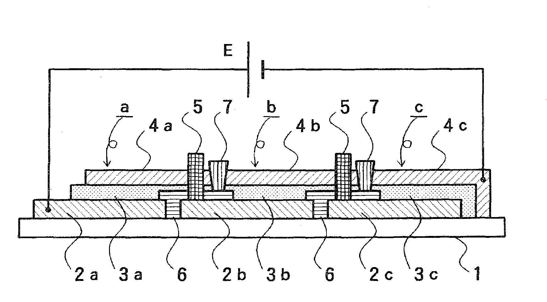
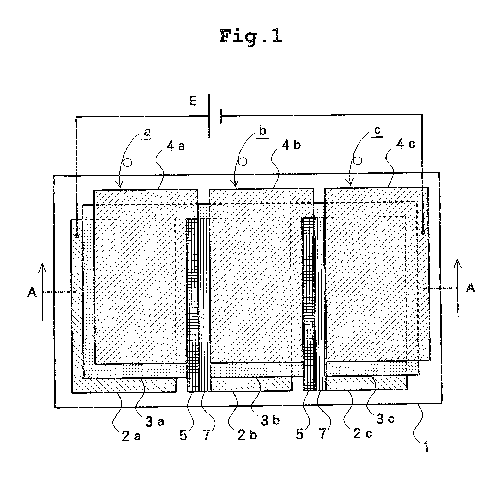
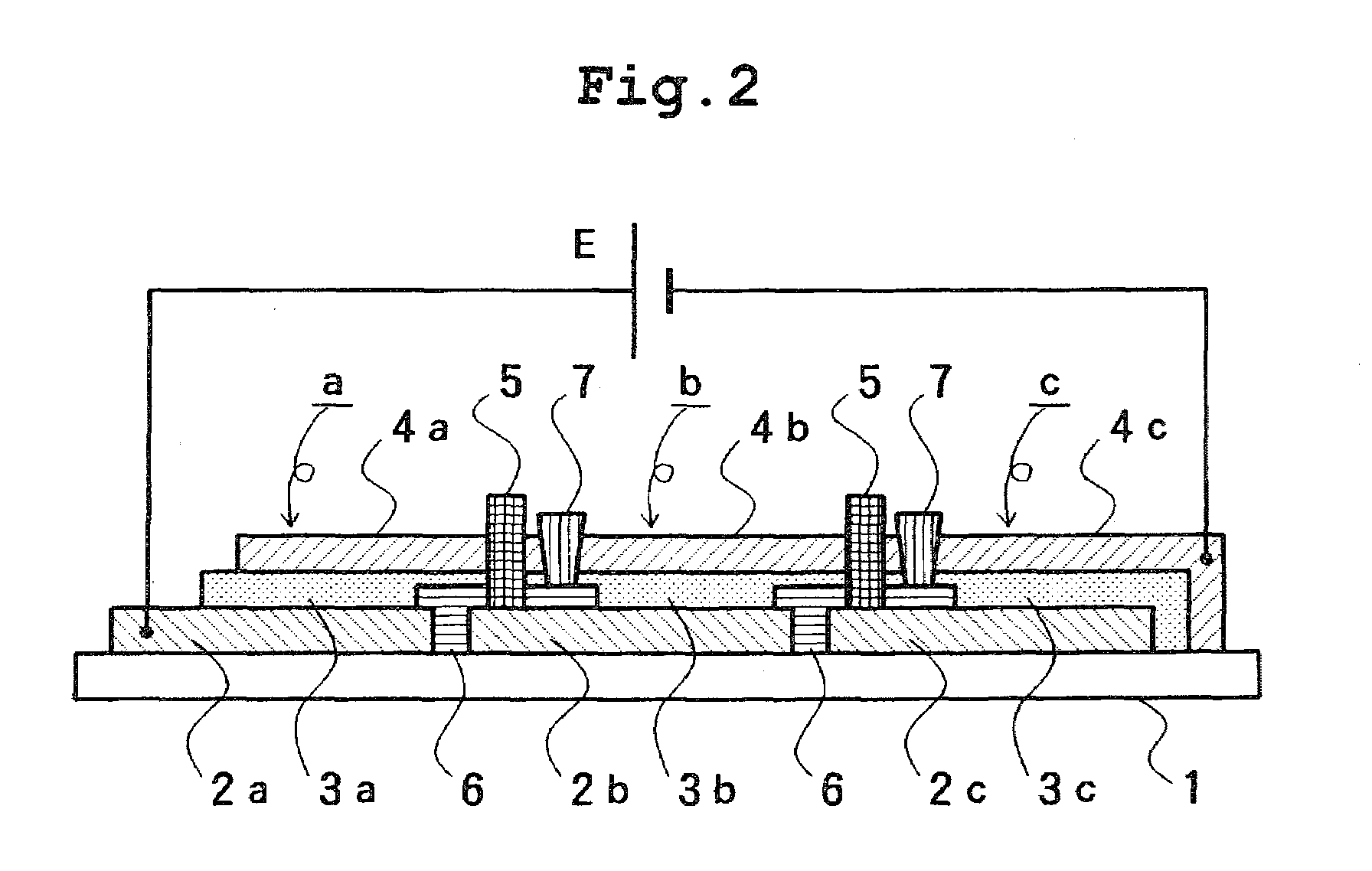
[0053]Hereinafter, an organic EL light emitting device according to the present invention is described based on the embodiments shown in the drawings. FIGS. 1 to 4 show the first embodiment. FIG. 1 is an overhead schematic view of a laminated structure example of an organic EL light emitting device provided with three-divided light-emitting segments. FIG. 2 is a cross-sectional view of the laminated structure example of the organic EL light emitting device as viewed from a line A-A in a direction of arrow in FIG. 1. FIGS. 3A to 3F are cross-sectional views showing the order of an example of a process for manufacturing (film-forming) the organic EL light emitting device shown in FIGS. 1 and 2. FIG. 4 is a partial enlarged cross-sectional view of a part surrounded by a chain line B in FIG. 3F. In each drawing to be explained herein after, components having the same function as the above-described components in FIG. 9 are represented by same numbers, and thus the detailed description i...


PUM


Abstract

An organic EL light emitting device, in which a plurality of divided light emitting segments are connected in series, is efficiently manufactured without separate coating of organic EL light emitting layers with the use of a vapor-deposition mask. Conductor parts 5 are respectively formed on first electrodes 2b and 2c in boundary parts of adjacent light emitting segments a, b and c. Organic light emitting layers 3a to 3c and second electrode 4a to 4c are respectively stacked on each of the first electrode 2a to 2c. The conductor part 5 has a function for electrically connecting the first electrodes and the second electrodes in the adjacent light emitting segments, whereby the light emitting segments are connected in series.

Description

BACKGROUND OF THE INVENTION[0001]1. Field of the Invention[0002]The present invention relates to an organic EL light emitting device using organic EL (electroluminescence) element which is a surface light emitting source having a relatively large area, and a method for manufacturing the organic EL light emitting device.[0003]2. Description of the Related Art[0004]An organic EL element is driven at a direct current low voltage, thus can provide a high light-emitting efficiency, and at the same time, can realize the reduction of the weight and thickness, whereby the organic EL element is used in a flat panel display (FPD) in some portable apparatuses and the like. In addition, there is provided one in which an organic EL element as a surface light emitting source is used for, for example, a backlight for a liquid crystal display element.[0005]Meanwhile, the organic EL element can provide each light emitting color of R (red), G (green) and B (blue) by the selection of a material used f...

Claims


Application Information

Patent Timeline
Patent Type & Authority Applications(United States)
IPC IPC(8): H01J1/62H01J9/02
CPCH01L27/3204H01L2251/568H01L51/5203H01L27/3246H10K59/86H10K59/122H10K50/805H10K71/861H01L23/4828H10N30/2044H10K50/11
Inventor KAWAI, TAKASHISUZUKI, JOJI
Owner YAMAGATA PROMOTIONAL ORG FOR INDAL TECH
Why Eureka
Try Eureka