
Solid-state imaging device

a solid-state imaging and imaging device technology, applied in the direction of radioation control devices, television system scanning details, television systems, etc., can solve the problems of color mixture, microlens forming cost, and increase in the thickness of the microlens as much as the thickness of the microlens

Active Publication Date: 2008-09-18
FUJIFILM CORP
View PDF7 Cites 47 Cited by
  • Summary
  • Abstract
  • Description
  • Claims
  • Application Information

AI Technical Summary

Benefits of technology

[0006]It is therefore an object of the invention to provide a solid-state imaging device including photoelectric conversion elements and color filters above a substrate for making it possible to prevent a color mixture caused by incident light in a slanting direction without providing any microlens on the top part.

Problems solved by technology

However, in the described solid-state imaging device, if there is incident light in a slanting direction, there is a possibility that light passing through the color filter of one pixel may be incident on the photoelectric conversion film of a pixel adjacent to that pixel, causing a color mixture to occur.
In this case, however, problems of the microlens forming cost, an increase in the thickness as much as that of the microlens, occurrence of brightness shading caused by the microlens, etc., occur.

Method used


Image

  • Solid-state imaging device
  • Solid-state imaging device
  • Solid-state imaging device

Examples


Embodiment Construction

[0031]Referring now to the accompanying drawings, there is shown an embodiment of the invention.

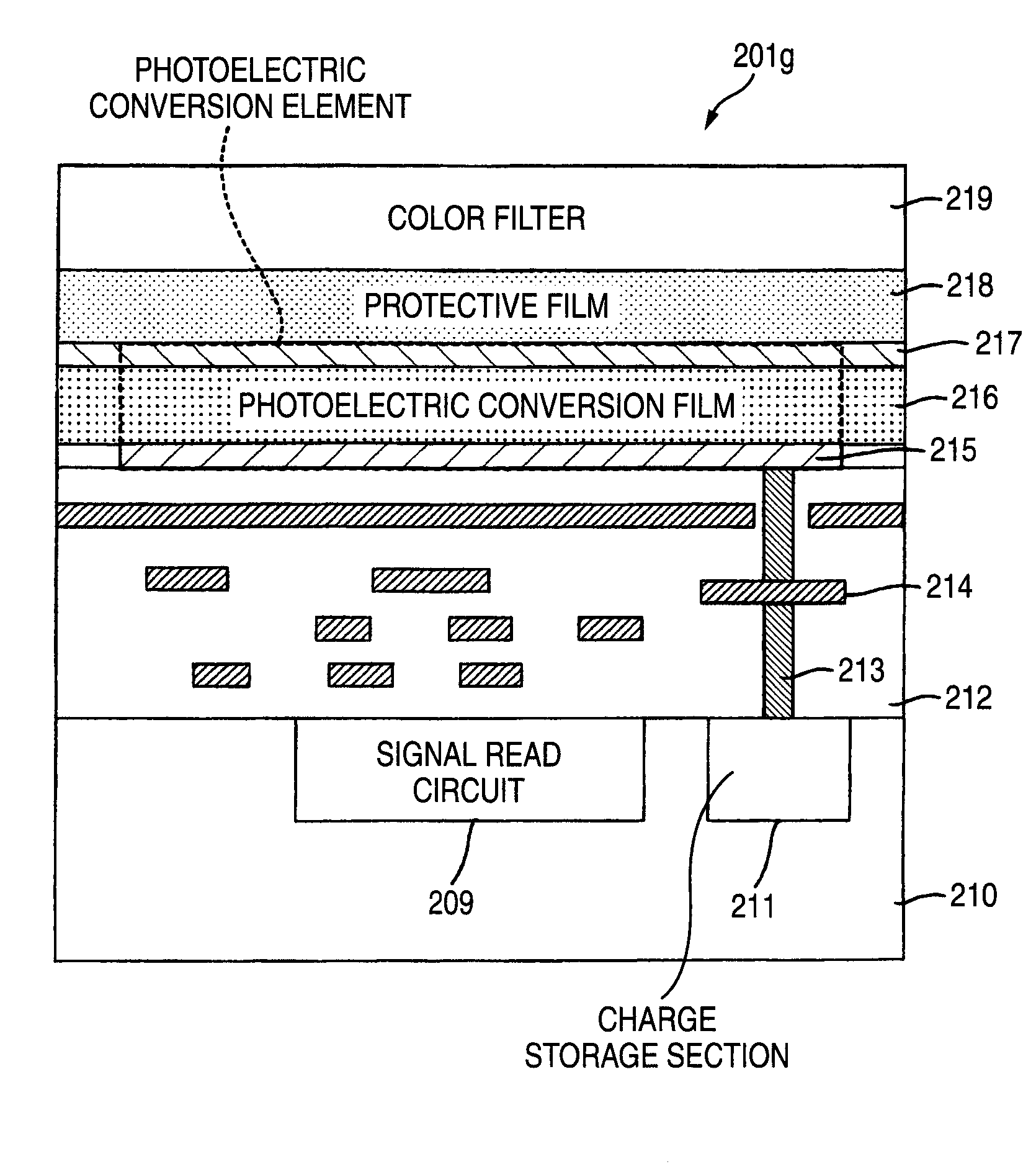
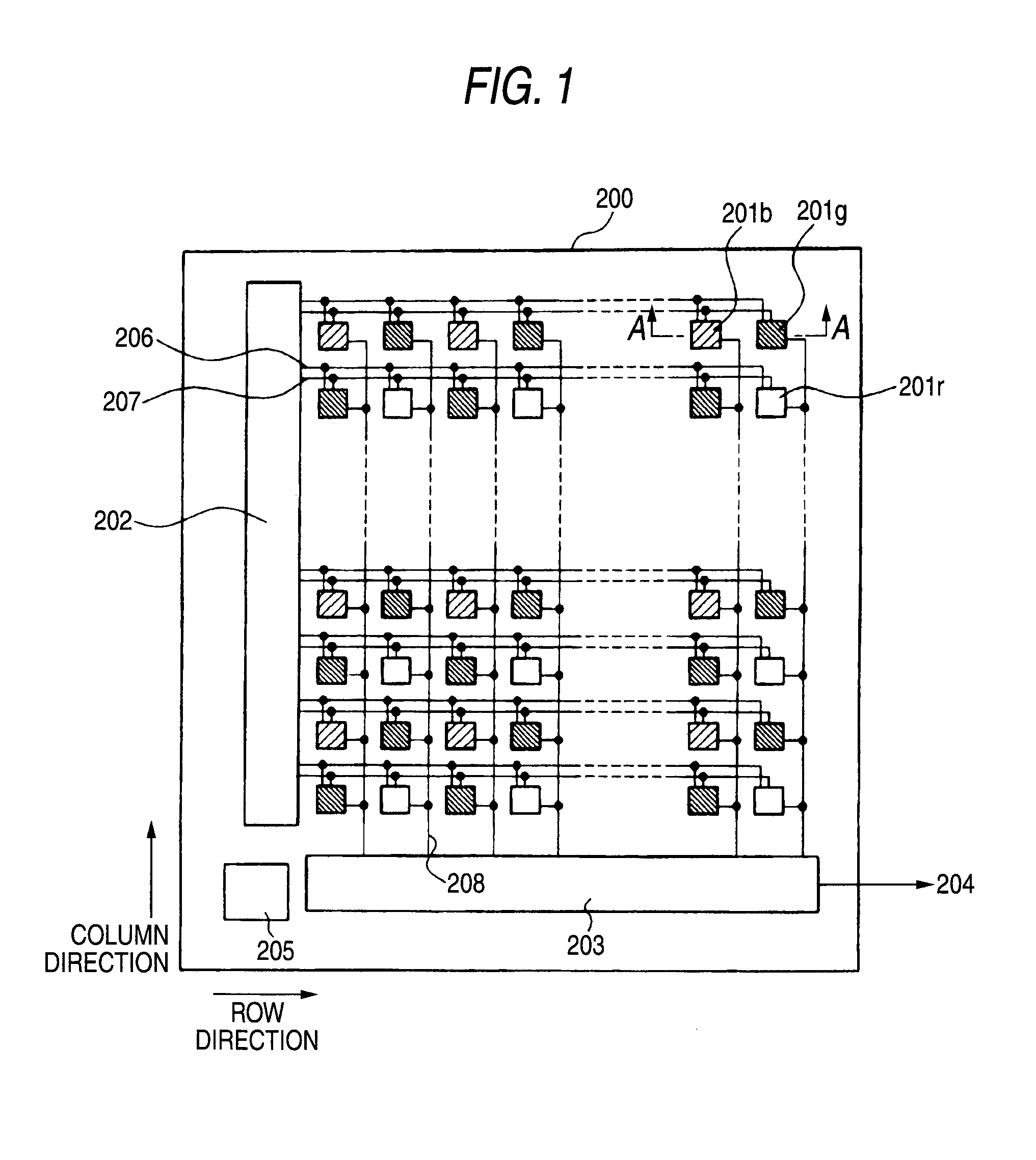
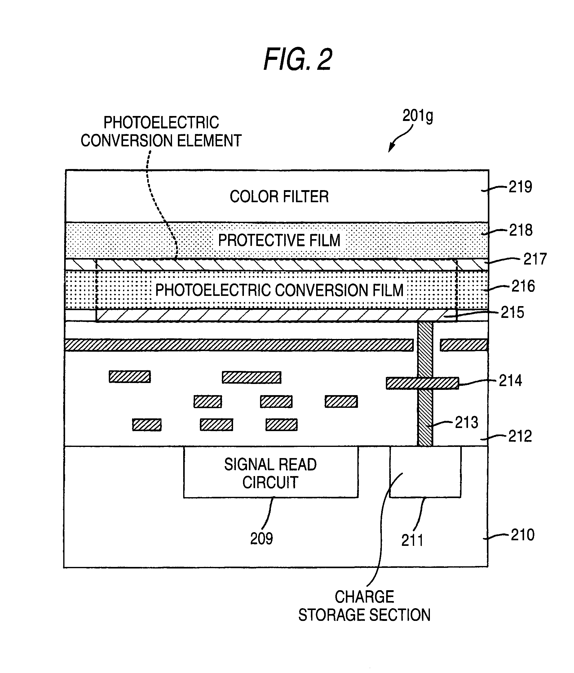
[0032]FIG. 1 is a surface schematic drawing to show the configuration of a solid-state imaging device to describe an embodiment of the invention. FIG. 2 is a sectional schematic drawing of one pixel part of the solid-state imaging device in FIG. 1.

[0033]A solid-state imaging device 200 shown in FIG. 1 includes a large number of pixel parts (201r, 201g, 201b) arranged like a tetragonal lattice in a row direction and a column direction orthogonal to the row direction in the same plane. The many pixel parts contain three types of pixel parts 201r for providing a color signal of a red component, pixel parts 201g for providing a color signal of a green component, and pixel parts 201b for providing a color signal of a blue component. As arrangement of the many pixel parts, a bg pixel part row of an alternating pattern of the pixel parts 201b and 201g in the row direction and a gr pixel part row...


PUM


Abstract

A solid-state imaging device comprising a plurality of pixel parts each capable of obtaining one color signal, said plurality of pixel parts being arranged in the same plane, wherein each of the pixel parts comprises: a photoelectric conversion element comprising a lower electrode formed on or above a substrate, an upper electrode formed above the lower electrode and a photoelectric conversion film sandwiched between the lower electrode and the upper electrode; and a color filter formed on or above the upper electrode, wherein d<p where d is a distance from a lower face of the photoelectric conversion film to an upper face of the color filter and p is an arrangement pitch of the photoelectric conversion element.

Description

BACKGROUND OF THE INVENTION[0001]1. Field of the Invention[0002]This invention relates to a solid-state imaging device wherein a plurality of pixel parts each capable of providing one color signal are arranged in the same plane.[0003]2. Description of the Related Art[0004]JP-T-2002-502120 discloses a solid-state imaging device of a configuration wherein a lower electrode is formed on a silicon substrate, a photoelectric conversion film made of an organic photoelectric conversion material is formed on the lower electrode, upper electrodes divided each for each pixel are formed on the photoelectric conversion film, and color filters divided for each pixel are formed on the upper electrodes in a one-to-one correspondence. According to such a solid-state imaging device, the light reception area of each pixel can be increased and higher sensitivity can be expected as compared with a single-plate solid-state imaging device which is mainstream at present. The whole silicon substrate can be...

Claims


Application Information

Patent Timeline
IPC IPC(8): H04N3/14H01L27/14H01L27/146H04N5/335H04N5/357H04N5/359H04N5/369H04N5/372H04N5/374
CPCH01L27/14621H01L27/14623H01L27/14632H04N5/335H01L27/14687H01L27/307H01L27/14667H04N25/00H10K39/32H01L27/146
Inventor GOTO, TAKASHI
Owner FUJIFILM CORP
Features
  • Generate Ideas
  • Intellectual Property
  • Life Sciences
  • Materials
  • Tech Scout
  • Unparalleled Data Quality
  • Higher Quality Content
  • 60% Fewer Hallucinations
Learn More