
Barrier dielectric stack for seam protection

a dielectric stack and barrier technology, applied in the field of metal oxide semiconductor field effect transistors, can solve problems such as short circuits of devices

Inactive Publication Date: 2008-09-18
IBM CORP
View PDF17 Cites 4 Cited by
  • Summary
  • Abstract
  • Description
  • Claims
  • Application Information

AI Technical Summary

Benefits of technology

[0009]When the second dielectric layer of the dielectric stack includes seams, the seams of the second dielectric are offset from the seams present in the first dielectric layer therefore providing a discontinuity in the electrical pathway within the deposited layers caused by the seams being aligned. By depositing multiple dielectric layers atop one another, any seams present in the dielectric layers are covered or offset from one another, therefore providing a conformal dielectric layered stack having a discontinuous electrical pathway. In the present invention, the passivation stack thus has discontinuous seams. The term “discontinuous seams” denotes that the seams of each dielectric layer within the conformal dielectric layered stack are covered or offset from one another in a manner that would substantially eliminate electrical paths between the gate conductor and contact of FET devices of current and future generations of scaling.
[0010]Broadly, the inventive semiconducting device comprises:a gate dielectric atop a semiconducting substrate, said semiconducting substrate containing source and drain regions adjacent said gate dielectric;a gate conductor atop said gate dielectric;a conformal dielectric passivation stack positioned on at least said gate conductor sidewalls, said conformal dielectric passivation stack containing a discontinuous electrical pathway; anda contact to said source and drain regions, wherein said conformal dielectric passivation stack substantially eliminates shorting between said contact and said gate conductor.

Problems solved by technology

This electrical path can, in turn, result in device shorting.

Method used


Image

  • Barrier dielectric stack for seam protection
  • Barrier dielectric stack for seam protection
  • Barrier dielectric stack for seam protection

Examples


Embodiment Construction

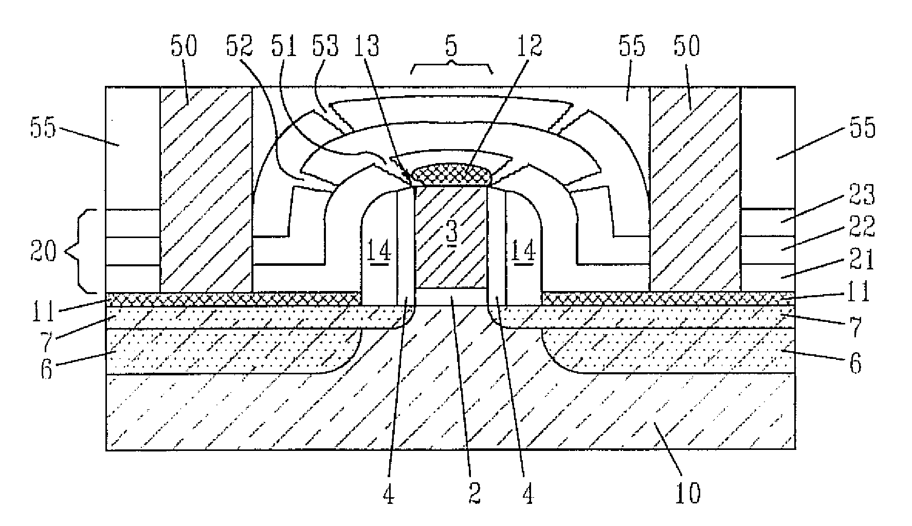
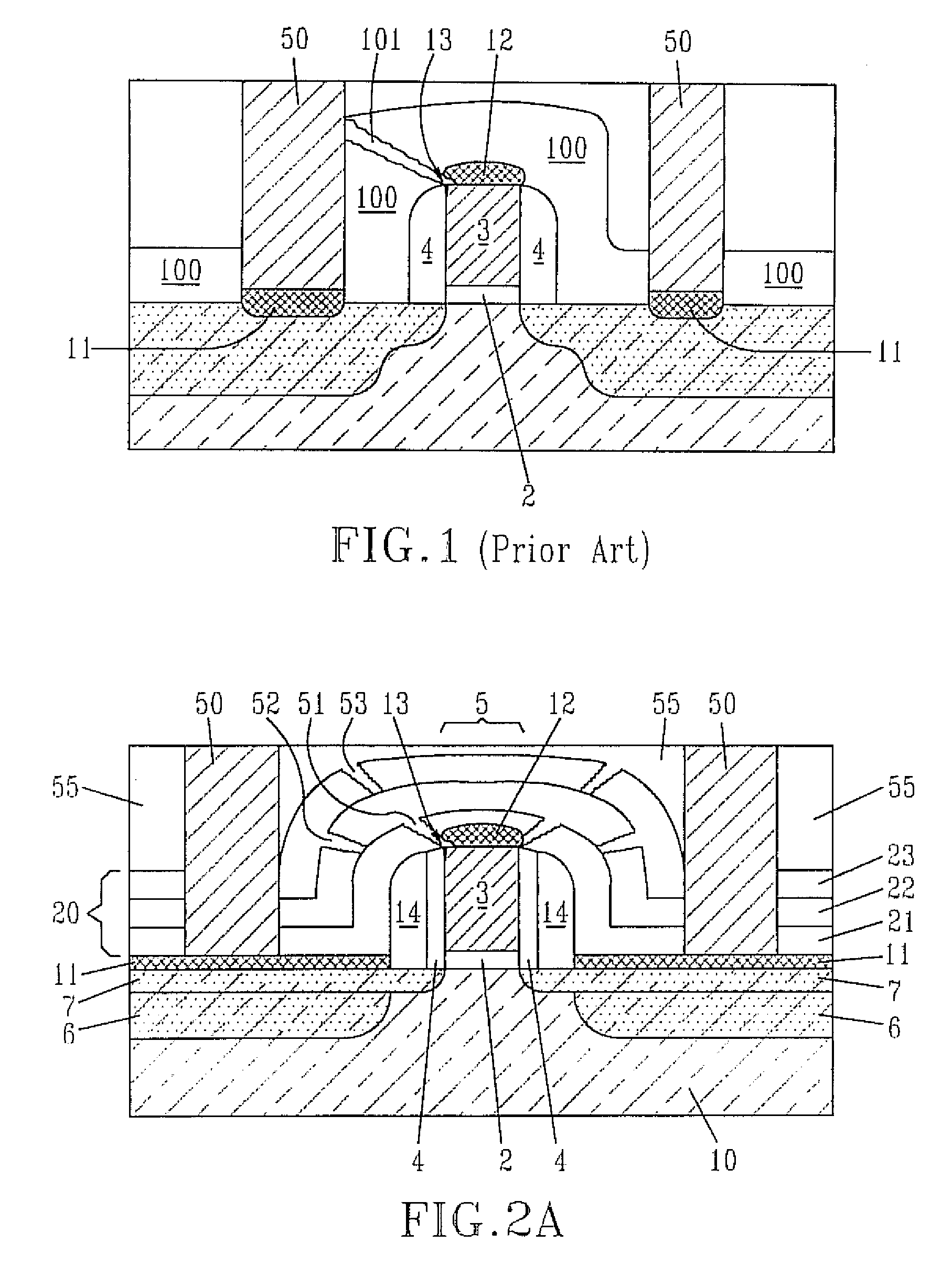
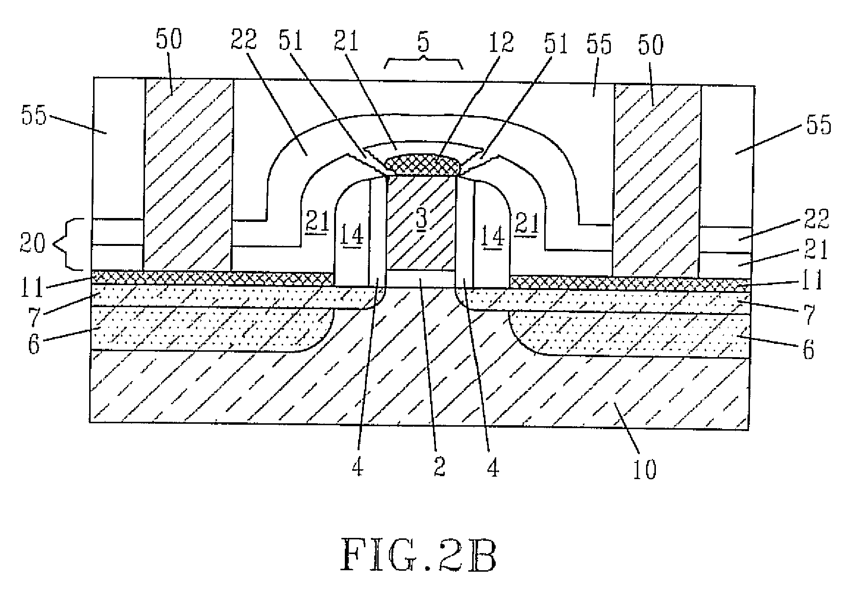
[0016]The present invention, which provides a method of passivating the gate conductor of a field effect transistor with a conformal dielectric passivation stack having discontinuous electrical pathways as well as the structure that is formed from the inventive method, will now be described in greater detail. It is noted that the drawings of the present application are provided for illustrative purposes and thus they are not drawn to scale. In particular, the dimensions of the seams and their relative position to each other have been enlarged to exemplify the present invention.

[0017]In the accompanying drawings, like and / or corresponding elements are referred to by like reference numbers. In the drawings, a single gate region is shown and described. Despite this illustration, the present invention is not limited to a structure including a single gate region. Instead, a plurality of such gate regions is contemplated.

[0018]Referring to FIG. 2A, in one embodiment of the present inventi...


PUM


Abstract

The present invention provides a semiconducting device including a gate dielectric atop a semiconducting substrate, the semiconducting substrate containing source and drain regions adjacent the gate dielectric; a gate conductor atop the gate dielectric; a conformal dielectric passivation stack positioned on at least the gate conductor sidewalls, the conformal dielectric passivation stack comprising a plurality of conformal dielectric layers, wherein no electrical path extends entirely through the stack; and a contact to the source and drain regions, wherein the discontinuous seam through the conformal dielectric passivation stack substantially eliminates shorting between the contact and the gate conductor. The present invention also provides a method for forming the above-described semiconducting device.

Description

RELATED APPLICATIONS[0001]This application is a divisional application of U.S. Ser. No. 10 / 904,661, filed Nov. 22, 2004.FIELD OF THE INVENTION[0002]The present invention relates to semiconductor devices having enhanced resistance to shorting, and more particularly to metal oxide semiconductor field effect transistors (MOSFETS), in which electrical shorting between the gate conductor and the contacts to the source and drain regions of the device is substantially eliminated by a conformal dielectric passivation stack positioned on at least the sidewalls of the gate region. The inventive conformal dielectric passivation stack comprises at least a first conformal dielectric layer and a second conformal dielectric layer in which no electrical pathway is present that extends entirely through the stack. The absence of the electrical pathway can be achieved by using a second conformal dielectric that is seamless or one in which the seams are offset from the seams present in the first dielec...

Claims


Application Information

Patent Timeline
Patent Type & Authority Applications(United States)
IPC IPC(8): H01L21/314
CPCH01L23/3192H01L29/495H01L29/4966H01L29/4975H01L29/665H01L29/6656H01L2924/0002H01L29/6659H01L2924/13091H01L2924/00H01L21/76832
Inventor ENGEL, BRETT H.LUCARINI, STEPHEN M.SYLVESTRI, JOHN D.WANG, YUN-YU
Owner IBM CORP
Learn More