Flat panel display and fabrication method thereof

a technology of flat panel display and fabrication method, which is applied in the direction of instruments, lighting and heating apparatus, semiconductor devices for light sources, etc., can solve the problem that the display cannot provide the desired brightness performance, and achieve the effect of promoting the brightness performance of the flat panel display and improving the optical usage efficiency

Inactive Publication Date: 2008-09-25
INNOLUX CORP
View PDF11 Cites 50 Cited by
  • Summary
  • Abstract
  • Description
  • Claims
  • Application Information

AI Technical Summary

Benefits of technology

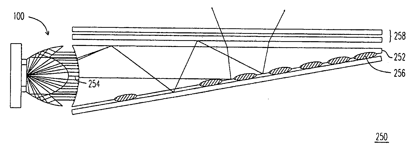
[0014]The present invention enables the light rays emitted from the light emitting semiconductor device collected within a convergent angle by design so as to make the divergent angle of the light rays provided by the light emitting device smaller. Therefore, the backlight module employing the light emitting device of the present invention has better optical usage efficiency, and thereby the present invention can provide the display panel with a high-luminance backlight module and promote the brightness performance of the flat panel display thereof.

Problems solved by technology

However, if a backlight module cannot provide a desired luminous efficiency, the backlight module cannot provide a desired brightness such that the display cannot provide a desired brightness performance.

Method used


Image

  • Flat panel display and fabrication method thereof
  • Flat panel display and fabrication method thereof
  • Flat panel display and fabrication method thereof

Examples


first embodiment

The First Embodiment

[0034]FIG. 4 is a diagram of a light emitting device according to the first embodiment of the present invention and FIG. 5 is a diagram illustrating a convergent angle of the light emitting device shown in FIG. 4. Referring to FIG. 4, a light emitting device 400 can include a light emitting semiconductor device 410 and a lens 420. The lens 420 is configured to cover the light emitting semiconductor device 410. The lens 420 can include two reflective surfaces 422, two refractive surfaces 424, and a Fresnel surface 426. Each reflective surface 422 is disposed at each side with respect to a central axis 421 of the lens 420. Each refractive surface 424 is connected with one of the reflective surfaces 422 and has a tilt included angle with respect to the central axis 421 (notated by θ1 and θ2 in FIG. 4). Each of the refractive surfaces 424 is extended from a place connecting with the reflective surface 422 along a direction toward the bottom of the lens 420 and / or the...

second embodiment

The Second Embodiment

[0045]FIG. 6 is an exploded diagram of a light emitting device according to the second embodiment of the present invention. In FIG. 6, a light emitting device 500 (No element associated with reference numeral 500 is shown in FIG. 6) can include a light emitting semiconductor device 510, a lens 520, and a circuit board 530. The light emitting semiconductor device 510 can be disposed over the circuit board 530. The circuit board 530 can be a metal core printed circuit board (MCPCB). The lens 520 is configured to cover the light emitting semiconductor device 510. The lens 520 can include two reflective surfaces 522, a plurality of refractive surfaces 524, and an accommodating recess 526. The reflective surfaces 522 can be disposed at both sides with respect to a central axis 521 of the lens 520. The refractive surfaces 524 can be disposed between the two reflective surfaces 522 and respectively have a tilt included angle with respect to the central axis 521 (notate...

third embodiment

The Third Embodiment

[0051]FIG. 9 is an exploded diagram of a light emitting device according to the third embodiment of the present invention. Referring to FIG. 9, a light emitting device 500c can be similar to the light emitting device 500 described above in conjunction with FIG. 6, except that the accommodating recess 526 of the lens 520c of the light emitting device 500c is a spherical recess, and the reflective surfaces 522 of the lens 520c are attached with a fixing frame 550. A plurality of positioning pins 554 can be disposed over the bottom of the fixing frame 550 and configured through a circuit board 530. In embodiments, the reflective surfaces 522 can be TIR surfaces, or a reflective layer can be applied between the reflective surfaces 522 and the fixing frame 550.

[0052]Since the accommodating recess 526 of the lens 520c is a spherical recess, the deformation of the accommodating recess 526 occurring after forming the lens 520c by using an inject moulding process can be d...


PUM

PropertyMeasurementUnit
convergent angleaaaaaaaaaa

Abstract

A flat panel display is provided. The flat panel includes at least one light emitting device having a light emitting semiconductor device and a lens. The lens includes two reflective surfaces which are disposed at both sides with respect to a central axis of the lens. Refractive surfaces connect with the respective reflective surfaces and have a tilt included angle with respect to the central axis. Each of the refractive surfaces continuously extends from the reflective surface along a direction toward the central axis. A Fresnel surface is configured between the refractive surfaces. Light rays emitted from the light emitting semiconductor device reach the lens. A portion of the light rays reaching each of the reflective surfaces is reflected to at least one of the refractive surfaces and the Fresnel surface. The reflected light rays are refracted and collected with a convergent angle.

Description

CROSS-REFERENCES TO RELATED APPLICATIONS[0001]This application claims the benefit of Taiwan application Serial No. 096109689, filed Mar. 21, 2007, the subject matter of which is incorporated herein by reference.BACKGROUND OF THE INVENTION[0002]The present invention generally relates to flat panel displays, and more particularly, to flat panel displays having at least one light emitting device having a small degree divergent angle and fabrication methods thereof.[0003]In recent years, display technologies have been developed significantly. After continuous research and development, products including liquid crystal displays (LCDs), plasma displays, and organic light emitting diode displays (OLED displays) in various sizes have been widely used in various industries. Furthermore, the development of the display technology has been directed toward manufacturing displays having high brightness and high yield for the industry to manufacture the products with more commercial values. Of all...

Claims


Application Information

Patent Timeline
Patent Type & Authority Applications(United States)
IPC IPC(8): F21V13/04G02F1/13357
CPCF21V5/04F21V5/045F21V7/0091F21Y2101/02G02B6/0018G02F2001/133607G02B6/003G02B6/0043G02B6/0051G02F1/133603G02F1/133605G02B6/002F21Y2115/10G02F1/133607
Inventor HUNG, CHEN-PIN
Owner INNOLUX CORP
Why Eureka
Try Eureka