

Sensor Product for Electric Field Sensing
a technology of sensor products and electric fields, applied in the direction of electric digital data processing, instruments, electrical apparatus, etc., can solve the problems of limited scalability for large areas, poor application for outdoor or harsh environments, and the generality of user interface devices that are relatively fragile and expensive. , to achieve the effect of high electrical conductivity
- Summary
- Abstract
- Description
- Claims
- Application Information
AI Technical Summary
Benefits of technology
Problems solved by technology
Method used
Image

Examples
example 1
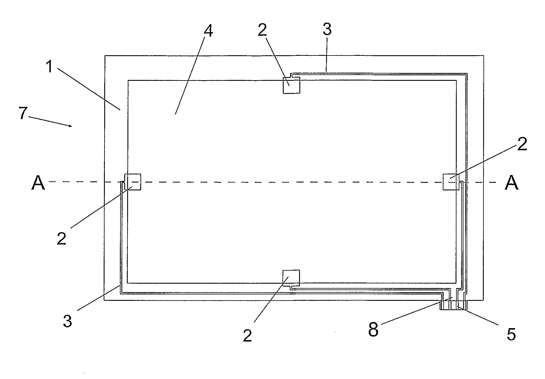
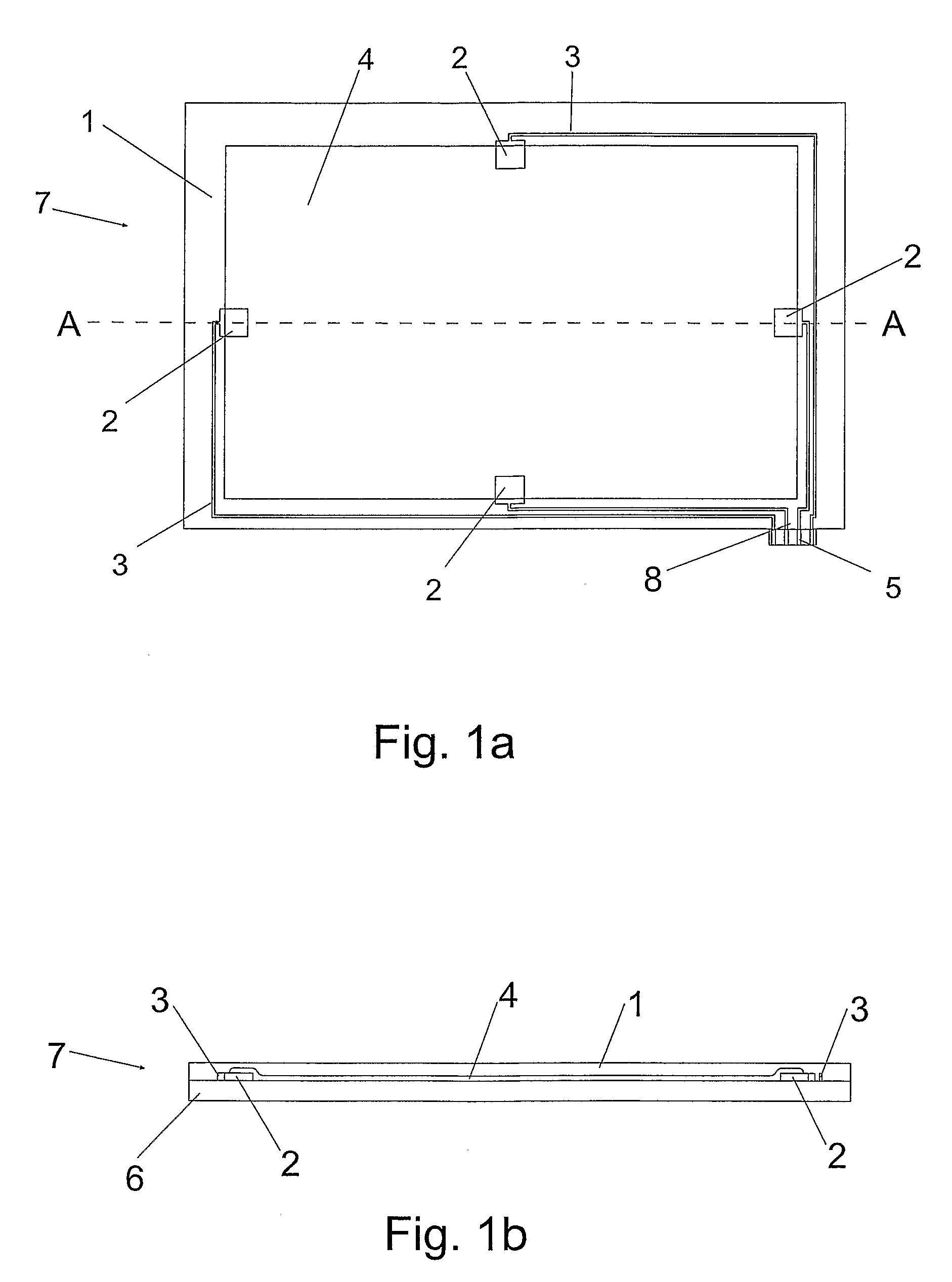
[0043]A sensor product according to FIG. 1 was manufactured. The electrodes and conductors of the sensor product are of aluminium, and the resistive sheet is a printed area. The electrically conductive element of the printing ink is carbon.
[0044]The manufacturing process of the sensor product comprises:[0045]1. The conductors and electrodes can be made by any known aluminum etching technique by using the following process:[0046]a. Resist printing i.e. printing a conductor / s and an electrode pattern / s to a Al / PET laminate (e.g. PET / adhesive / aluminium) with a resist ink (e.g. Coates XV1000-2).[0047]b. Etching of the Al / PET laminate[0048]2. A resistive sheet is printed by using conducting carbon ink (e.g. Dupont 7102) on top of the etched PET—film. The conductivity of the carbon ink can be adjusted to the desired level by using dielectric paste (e.g. Dupont 3571). According to the research results, optimal resistance with a 141×225 mm size sheet is 0.9-1.1 MΩ, measured between two elec...
example 2
[0056]A sensor product according to FIG. 1 was manufactured. Electrodes and conductors of the sensor product are of copper, and the resistive sheet is a printed area. The electrically conductive element of the printing ink is carbon.
[0057]Manufacturing steps:[0058]1. Conductors and electrodes can be made by any known copper etching technique by using the following process steps:[0059]a. Resist printing i.e. printing conductor and electrode pattern on the copper PET laminate with resist ink (e.g. Coates XV1000-2).[0060]b. Etching of copper laminate (e.g. PET—adhesive—copper).[0061]2. Resistive area (the resistive sheet) is printed by using electrically conductive carbon ink (e.g. Dupont 7102) on top of the etched PET—film. The conductivity of the carbon ink can be adjusted to the desired level by using a dielectric paste (e.g. Dupont 3571). According to the research results, optimal resistance with a 141×225 mm size sheet is 0.9-1.1 MΩ, measured between two electrodes at opposite sid...
example 3
[0070]A sensor product according to FIG. 1 was manufactured. Electrodes and conductors of the sensor product are printed with a silver ink, and the resistive sheet is a printed area. The electrically conductive element of the printing ink is carbon.
[0071]Manufacturing steps:[0072]1. Conductors and electrodes are printed with conducting silver ink on the substrate (e.g. PET film)[0073]2. A resistive sheet area is printed by using conducting carbon ink (e.g. Dupont 7102) on top of the etched PET—film. Conductivity of the carbon ink can be adjusted to the desired level by using dielectric paste (e.g. Dupont 3571). According to the research results, optimal resistance with a 141×225 mm size sheet is 0.9-1.1 MΩ, measured between two electrodes at opposite sides of the sheet in the length direction. The resistance may vary from 10 kΩ to 100 MΩ depending on the size of the sheet and the application). The carbon printed area overlaps with the silver electrodes.[0074]3. Lamination of a prote...
PUM
 Abstract
Description
Claims
Application Information