Method and device for driving solid-state imaging device, imaging apparatus, and image synthesizing method

a solid-state imaging and imaging apparatus technology, applied in the direction of still video cameras, radiation controlled devices, television systems, etc., can solve the problems of difficult to improve the saturation signal amount as compared with the sensitivity, image having appropriate gradation cannot be obtained, and speed becomes low, so as to achieve a wide dynamic range

Inactive Publication Date: 2008-10-02
FUJIFILM CORP
View PDF6 Cites 27 Cited by
  • Summary
  • Abstract
  • Description
  • Claims
  • Application Information

AI Technical Summary

Benefits of technology

[0010]An object of an illustrative, non-limiting embodiment of the invention is to provide a method and device for driving a solid-state imaging device, an imaging apparatus, and an image s

Problems solved by technology

To overcome sensitivity degradation, a microlens is formed on a surface and the light gathering efficiency per pixel is improved, but it is difficult to improve the saturation signal amount as compared with the sensitivity.
Thus, the saturation signal amount becomes insufficient relative to the sensitivity and in actual photographing, each pixel eas

Method used


Image

  • Method and device for driving solid-state imaging device, imaging apparatus, and image synthesizing method
  • Method and device for driving solid-state imaging device, imaging apparatus, and image synthesizing method
  • Method and device for driving solid-state imaging device, imaging apparatus, and image synthesizing method

Examples


first embodiment

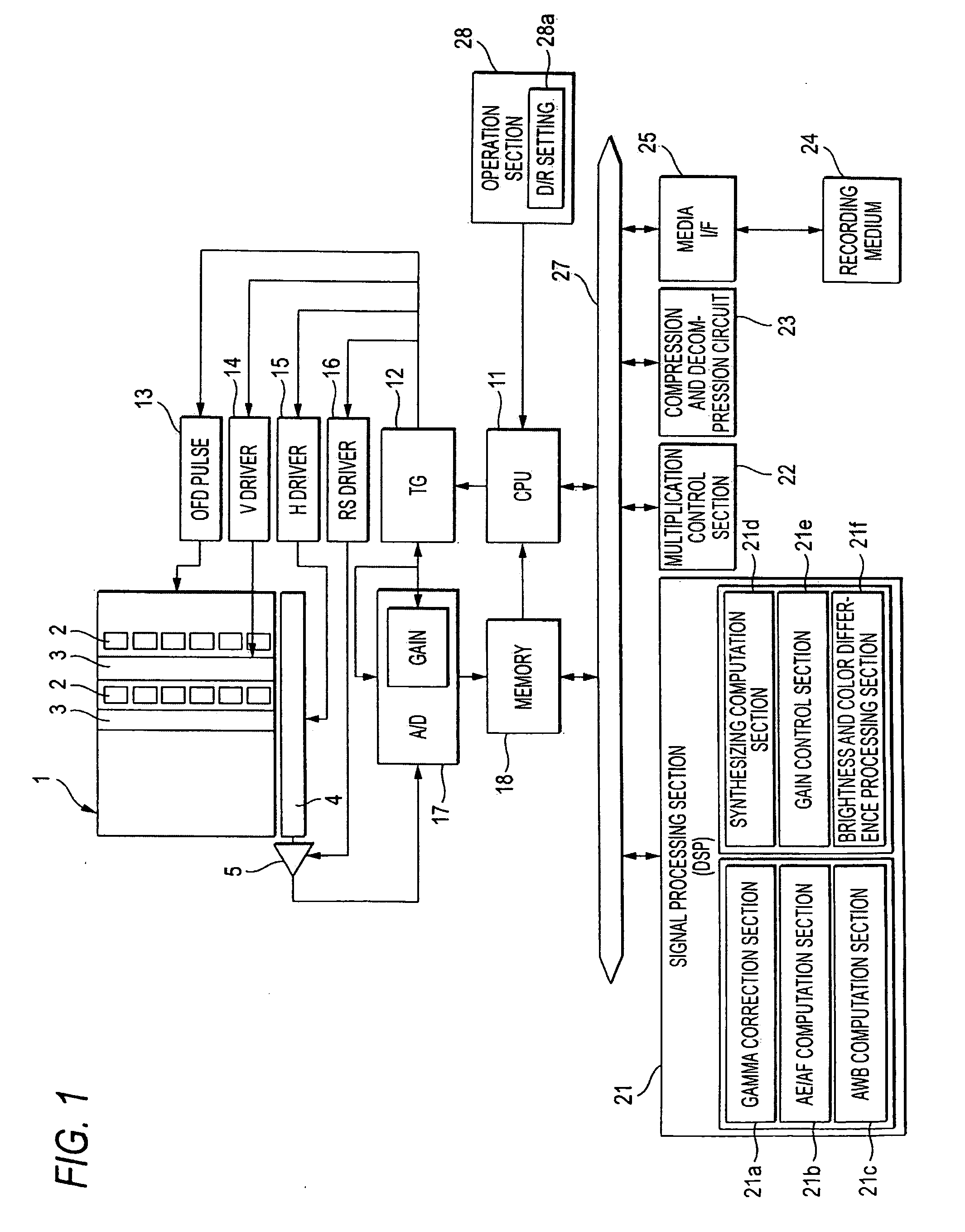
[0070]FIG. 6 is a schematic representation of a method for driving a solid-state imaging device according to a second exemplary embodiment of the invention. In the first embodiment, the vertical charge transfer path is driven in electron multiplication so as to multiply one image data to be synthesized. It is also possible to execute an electron multiplication at a time reading signal charges into vertical charge transfer path 3 from photodiode 2, instead of performing an electron multiplication in the vertical charge transfer path. For example, JP-A-5-335549 discloses performing an electron multiplication at a time reading charges from the photodiode.

[0071]To read signal charges into the vertical charge transfer path 3 from the photodiode 2, the shorter the gate length and the larger the read pulse amplitude, the steeper is the potential gradient formed between the photodiode 2 and the vertical charge transfer path 3. The electron multiplication factor is proportional to the potent...

fourth embodiment

[0079]In the fourth embodiment, signal charges transferred from each end part of the vertical charge transfer path 3 to a position off the end part are transferred to an output amplifier 5 while an electron multiplication of the signal charges is performed at each stage in the electron multiplication transfer path 62. Although the electron multiplication factor per stage is small as 1% to 2%, the signal charges are transferred and multiplied at 50 to 100 stages, whereby the electron multiplication factor can be made double or triple. Of course, the electron multiplication factor also changes according to the amplitude of an electron multiplication pulse.

[0080]In the embodiment, a plurality of pieces of image data, which is data of an image of the same scene taken and which is different in electron multiplication factor, can be synthesized, thereby providing an image with the dynamic range enlarged.

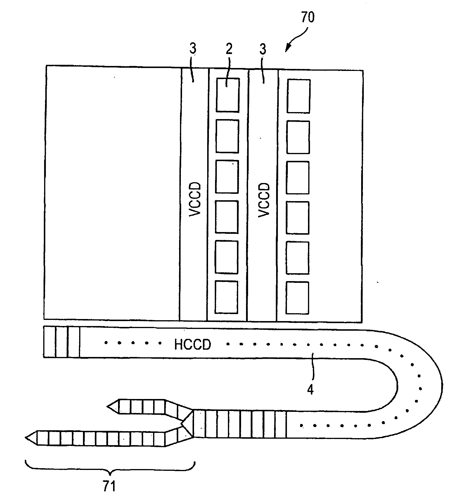
[0081]FIG. 9 is a surface schematic drawing of a solid-state imaging device 70 having ...


PUM


Abstract

A method for driving a solid-state imaging device including a plurality of pixels arranged in a two-dimensional array, each of the plurality of pixels accumulating a signal charge according to an amount of incident light, is provided. The method includes: performing electron multiplication of a first signal charge at a first multiplication factor to output a first image signal; and performing electron multiplication of a second signal charge at a second multiplication factor to output a second image signal, at least the first and second image signals being image signals of the same scene of a subject and being successively output.

Description

[0001]This application is based on and claims priority under 35 U.S.C. §119 from Japanese Patent Application No. 2007-94675 filed Mar. 30, 2007, the entire disclosure of which is herein incorporated by reference.BACKGROUND OF THE INVENTION[0002]1. Field of the Invention[0003]This invention relates to a method and device for driving a solid-state imaging device, an imaging apparatus, and an image synthesizing method in the imaging apparatus, which are capable of taking an image in a wide dynamic range.[0004]2. Description of Related Art[0005]JP-A-6-141229 discloses an example of a camera for taking an image in a wide dynamic range. In JP-A-6-141229, an overexposure image and an underexposure image of the same subject are continuously taken and are synthesized to widen the dynamic range of the image.[0006]In JP-A-59-210775, a solid-state imaging device is provided with both low-sensitivity pixels and high-sensitivity pixels, and low-sensitivity image data taken with the low-sensitivit...

Claims


Application Information

Patent Timeline
IPC IPC(8): H04N5/335H01L27/148H04N5/355H04N5/369H04N5/3728H04N5/374H04N5/376H04N101/00
CPCH04N3/1537H04N3/1575H04N5/2355H04N5/35572H04N5/37213H04N5/3728H04N23/741H04N25/587H04N25/57H04N25/713H04N25/73
Inventor OSHIMA, HIROYUKIKOBAYASHI, HIROKAZU
Owner FUJIFILM CORP
Why Eureka
Try Eureka