In-plane switching mode liquid crystal display panel and method for fabricating the same

a liquid crystal display panel and switching mode technology, applied in non-linear optics, instruments, optics, etc., can solve the problems of reducing process efficiency, reducing process efficiency, and reducing process efficiency

Active Publication Date: 2008-10-02
LG DISPLAY CO LTD
View PDF3 Cites 21 Cited by
  • Summary
  • Abstract
  • Description
  • Claims
  • Application Information

AI Technical Summary

Benefits of technology

[0020]Accordingly, the present invention is directed to an in-plane switching mode liquid crystal display panel and a method fo

Problems solved by technology

Such a TN mode LCD device has an advantage of a high aspect ratio, but has a drawback of a narrow viewing angle of

Method used


Image

  • In-plane switching mode liquid crystal display panel and method for fabricating the same
  • In-plane switching mode liquid crystal display panel and method for fabricating the same
  • In-plane switching mode liquid crystal display panel and method for fabricating the same

Examples


Embodiment Construction

[0045]Reference will now be made in detail to the preferred embodiments of the present invention, examples of which are illustrated in the accompanying drawings. Wherever possible, the same reference numbers will be used throughout the drawings to refer to the same or like parts.

[0046]First, the configuration and operation of a semi-transmissive in-plane switching (IPS) mode liquid crystal display (LCD) panel according to the present invention will be described with reference to FIGS. 5 and 6.

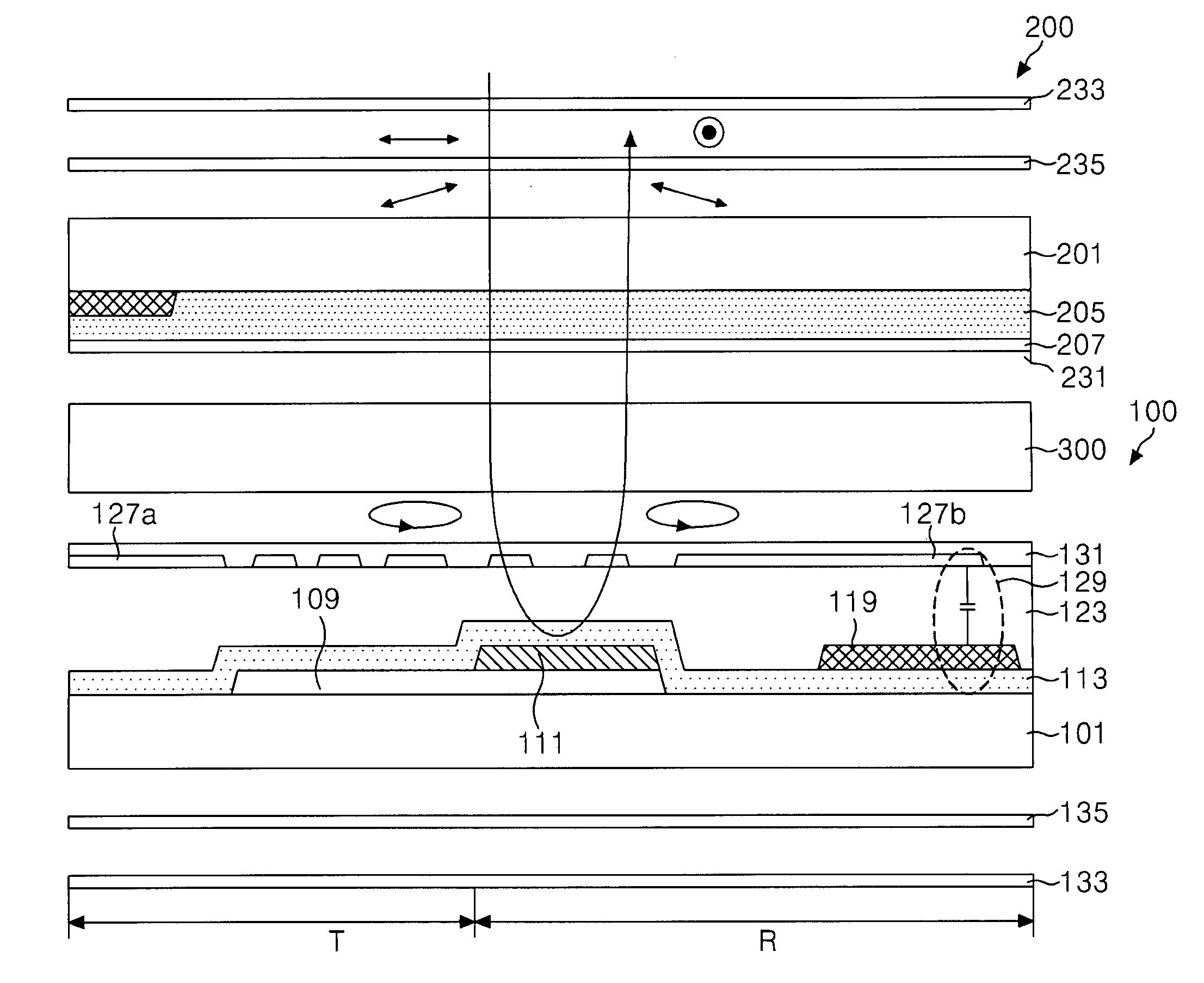
[0047]As shown in FIG. 5, the semi-transmissive IPS mode LCD panel 1000 includes a thin film transistor (TFT) substrate 100 formed with a plurality of lines and a plurality of TFTs, a color filter substrate 200 arranged to face the TFT substrate 100, and formed with color filters such that the color filters correspond to respective pixel regions, and a liquid crystal layer 300 dispensed in a cell gap defined between the two substrates 100 and 200, and oriented in a certain direction.

[0048]As sh...


PUM


Abstract

A semi-transmissive in-plane switching (IPS) mode liquid crystal display (LCD) panel, in which each pixel region can exhibit the same luminance in transmissive and reflective portions thereof while having a single cell gap structure, is disclosed. A method for fabricating the semi-transmissive IPS mode LCD panel is also disclosed. The panel, in which each pixel region includes a transmissive portion and a reflective portion, comprises a color filter substrate, a thin film transistor substrate assembled with the color filter substrate such that a cell gap is defined between the thin film transistor substrate and the color filter substrate, the thin film transistor substrate including storage capacitors each forming, in the reflective portion of an associated one of the pixel regions, a horizontal electric field different from a horizontal electric field formed in the transmissive portion of the associated pixel region, to compensate for a phase difference generated in the associated pixel region, and a liquid crystal layer dispensed in the cell gap, and oriented in a predetermined direction.

Description

[0001]This application claims the benefit of the Korean Patent Application No. 2007-030336, filed on Mar. 29, 2007, which is hereby incorporated by reference as if fully set forth herein.BACKGROUND OF THE INVENTION[0002]1. Field of the Invention[0003]The present invention relates to a semi-transmissive in-plane switching mode liquid crystal display panel and a method for fabricating the same, and more particularly, to a semi-transmissive in-plane switching mode liquid crystal display panel, in which each pixel region can exhibit the same luminance in transmissive and reflective portions thereof while having a single cell gap structure, and a method for fabricating the same.[0004]2. Discussion of the Related Art[0005]Liquid crystal display (LCD) devices display an image by adjusting the light transmittance of liquid crystals. Such LCD devices are classified into a twisted nematic (TN) mode and an in-plane switching (IPS) mode.[0006]In a TN mode LCD device, a common electrode formed o...

Claims


Application Information

Patent Timeline
IPC IPC(8): G02F1/1333G02F1/1335
CPCG02F1/133555G02F1/13363G02F1/134363G02F2001/133519G02F1/133519G02F1/1343G02F1/1335
Inventor JIN, HYUN SUK
Owner LG DISPLAY CO LTD
Why Eureka
Try Eureka