Array substrate for liquid crystal display device and manufacturing method of the same

Active Publication Date: 2008-10-02
LG DISPLAY CO LTD
View PDF4 Cites 27 Cited by
  • Summary
  • Abstract
  • Description
  • Claims
  • Application Information

AI Technical Summary

Benefits of technology

[0029]An advantage of the present invention is to provide an array substrate for an LCD device and a manufacturing method of the same that have uniform image qualities.

Problems solved by technology

At this time, there is high possibility that light leakage occurs due to alignment margins.
However, even though the COA-IPS mode LCD device has a larger aperture ratio and wide viewing angles, hand-shaped speckles may occur due to the color filter patterns.

Method used


Image

  • Array substrate for liquid crystal display device and manufacturing method of the same
  • Array substrate for liquid crystal display device and manufacturing method of the same
  • Array substrate for liquid crystal display device and manufacturing method of the same

Examples


first embodiment

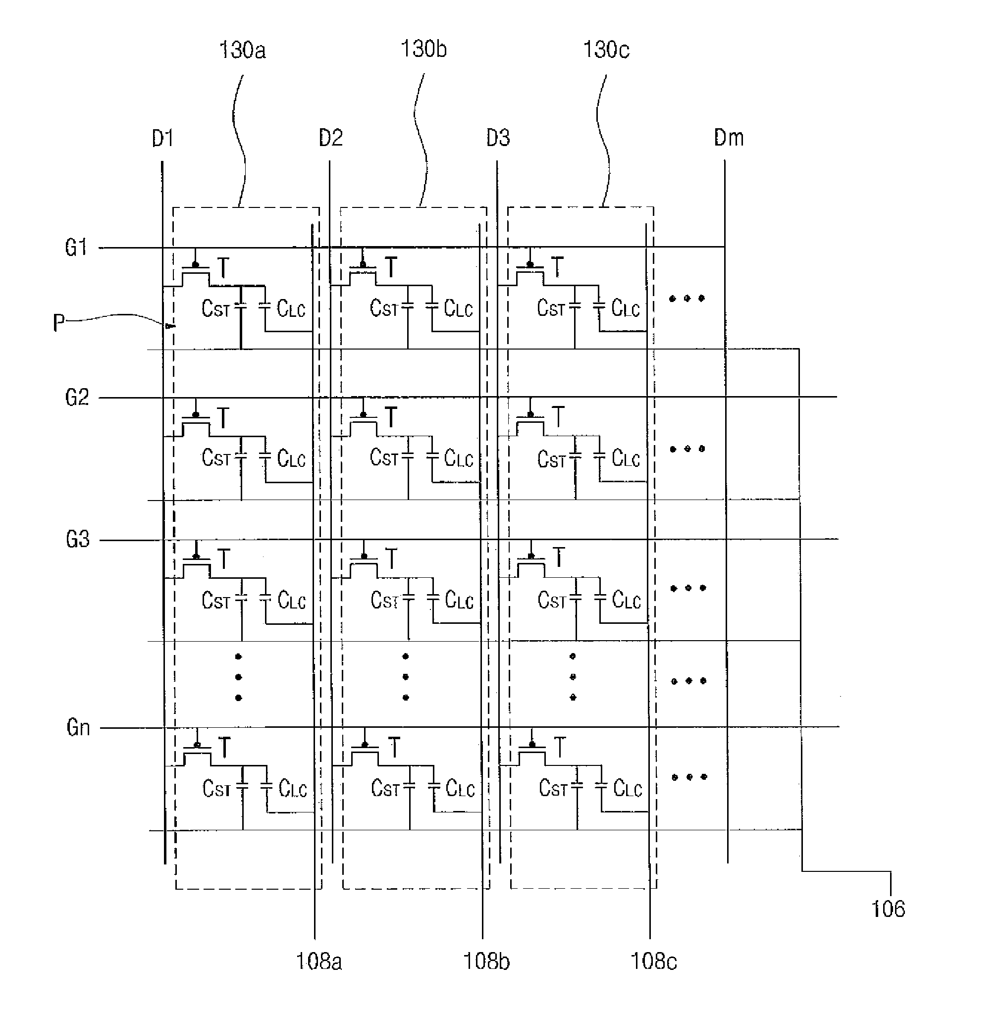
[0048]FIG. 5 is an equivalent circuit of an LCD device according to the present invention.

[0049]In FIG. 5, gate lines G1, G2, G3 to Gn (n is a natural number) are formed along a first direction and spaced apart from each other. Data lines D1, D2, D3 to Dm (m is a natural number) are formed along a second direction and cross the gate lines G1, G2, G3 to Gn to define pixel regions P.

[0050]A thin film transistor T, a liquid crystal capacitor CLC and a storage capacitor CST are formed at each pixel region P. The thin film transistor T is connected to a corresponding gate line G1, G2, G3 or Gn and a corresponding data line D1, D2, D3 to Dm. The storage capacitor CST is connected to the liquid crystal capacitor CLC substantially in parallel.

[0051]A color filter layer 130a, 130b and 130c is formed in each pixel region P such that one color corresponds to one pixel region P. Here, the color filter layer 130a, 130b and 130c is a stripe type in which color filter patterns along the second dir...

second embodiment

[0067]FIG. 7 is an equivalent circuit of an LCD device according to the present invention.

[0068]In FIG. 7, gate lines G1, G2, G3 to Gn (n is a natural number) are formed along a first direction and spaced apart from each other. Data lines D1, D2, D3 to Dm (m is a natural number) are formed along a second direction and cross the gate lines G1, G2, G3 to Gn to define pixel regions P.

[0069]A thin film transistor T, a liquid crystal capacitor CLC and a storage capacitor CST are formed at each pixel region P. The thin film transistor T is connected to a corresponding gate line G1, G2, G3 or Gn and a corresponding data line D1, D2, D3 or Dm. The storage capacitor CST is connected to the liquid crystal capacitor CLC substantially in parallel.

[0070]A color filter layer 230a, 230b and 230c is formed in each pixel region P such that one color corresponds to one pixel region P. Here, the color filter layer 230a, 230b and 230c is a stripe type in which color filter patterns along the second dir...

third embodiment

[0076]FIG. 8 is a schematic view of illustrating an array substrate for an LCD device according to the present invention. The LCD device is a COA type, in which a color filter layer is formed on the array substrate.

[0077]In FIG. 8, red, green and blue color filter patterns 324a, 324b and 324c are formed over a substrate 300. A common electrode 328 is formed on each of the red, green and blue color filter patterns 324a, 324b and 324c. A pixel electrode 334b is formed over the common electrode 328. The pixel electrode 334b overlaps the common electrode 328.

[0078]When voltages are applied to the common electrode 328 and the pixel electrode 334b, an electric field is induced between the common electrode 328 and the pixel electrode 334b. At this time, even though charges are induced in the color filter patterns 324a, 324b and 324c, the charges may be screened by the common electrode 328 and may not affect pixels corresponding to respective colors. Accordingly, the pixels can be uniformly...


PUM


Abstract

According to an embodiment, an array substrate for an LCD device includes a substrate, gate lines on the substrate along a first direction, data lines formed along a second direction and crossing the gate lines to define first, second and third pixel regions, thin film transistors at crossing points of the gate lines and the data lines, red, green and blue color filter patterns sequentially disposed in the first, second and third pixel regions, respectively, first, second and third common lines corresponding to the first, second and third pixel regions and receiving first, second and third common voltages, respectively, a pixel electrode over each of the red, green and blue color filter patterns and connected to one of the thin film transistors, and a common electrode over each of the red, green and blue color filter patterns and connected to one of the first, second and third common lines.

Description

[0001]The present application claims the priority benefits of Korean Patent Application Nos. 10-2007-0032220 filed in Korea on Apr. 2, 2007 and 10-2007-0037256 filed in Korea on Apr. 17, 2007, which are hereby incorporated by reference for all purposes as if fully set forth herein.BACKGROUND OF THE INVENTION[0002]1. Field of the Invention[0003]The present invention relates to a liquid crystal display (LCD) device, and more particularly, to an array substrate for a liquid crystal display device and a manufacturing method of the same.[0004]2. Discussion of the Related Art[0005]Liquid crystal display (LCD) devices are driven based on optical anisotropy and polarization characteristics of a liquid crystal material. Liquid crystal molecules have a long and thin shape, and the liquid crystal molecules are regularly arranged along in an alignment direction. Light passes through the LCD device along the long and thin shape of the liquid crystal molecules. The alignment of the liquid crystal...

Claims


Application Information

Patent Timeline
IPC IPC(8): G02F1/1333G02F1/1335
CPCG02F1/133371G02F1/134363G02F2001/136222G02F2201/121G09G3/3607G09G3/3648G09G3/3655G09G2300/0876G02F1/136222
Inventor CHAE, GEE-SUNG
Owner LG DISPLAY CO LTD
Why Eureka
Try Eureka