

Magneto-resistance effect element, magnetic head, magnetic recording/reproducing device and method for manufacturing a magneto-resistance effect element
a technology of resistance effect and magnetic head, which is applied in the field of magnetic head, magnetic recording/reproducing device and method for manufacturing a magnetoresistance effect element, to achieve the effect of reducing the surface roughness of the bottom electrod
- Summary
- Abstract
- Description
- Claims
- Application Information
AI Technical Summary
Benefits of technology
Problems solved by technology
Method used
Image

Examples
example 1
[0077]Example 1 relating to the magneto-resistance effect element 10 will be described. In Example 1, the magneto-resistance effect element 10 was formed as follows:
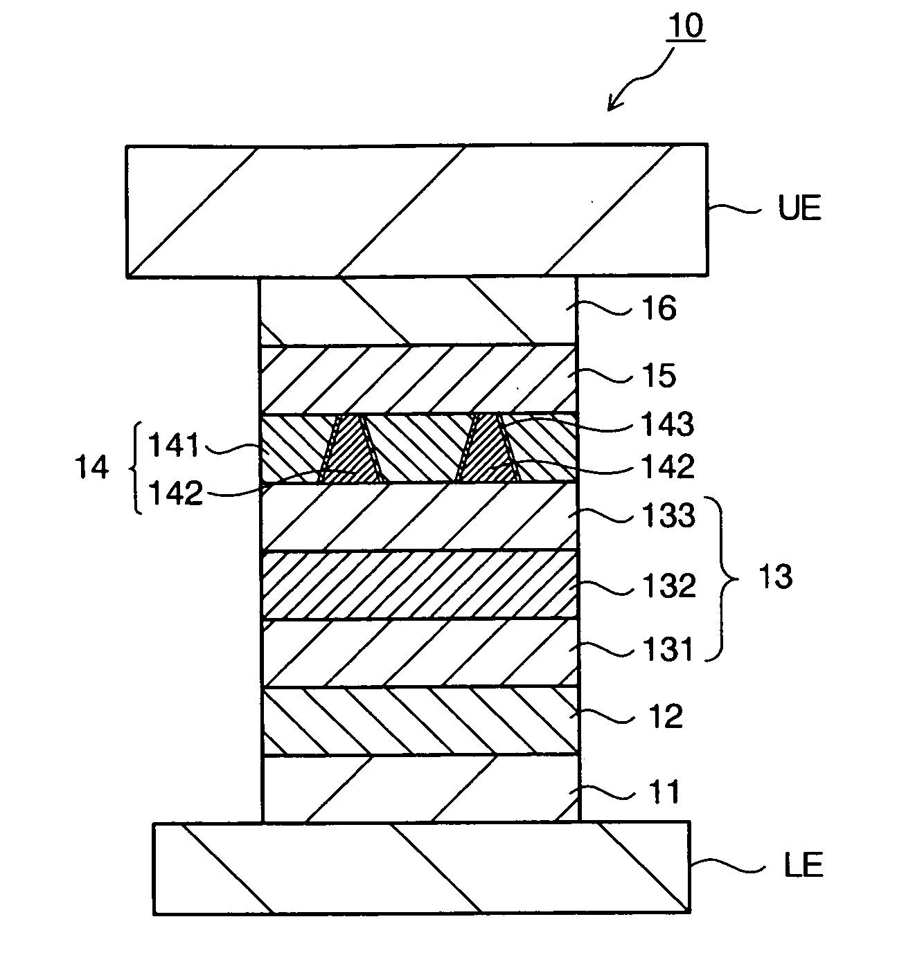
[0078]Underlayer 11: Ta 5 nm / NiFeCr 7 nm
[0079]Antiferromagnetic layer 12: PtMn 15 nm
[0080]First pinned layer 131: Co9Fe1 3.3 nm
[0081]Antiparallel magnetic coupling layer 132: Ru 0.9 nm
[0082]Second pinned layer 132: Fe5CO5 2.5 nm
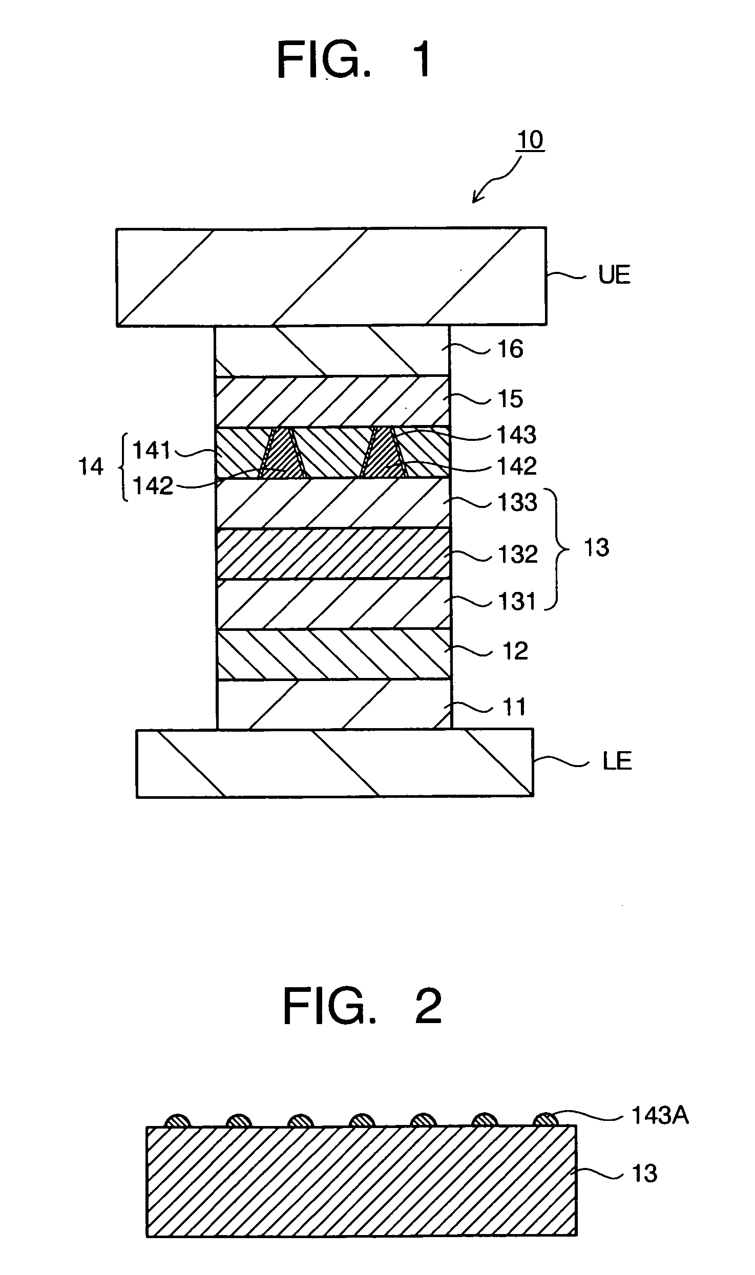
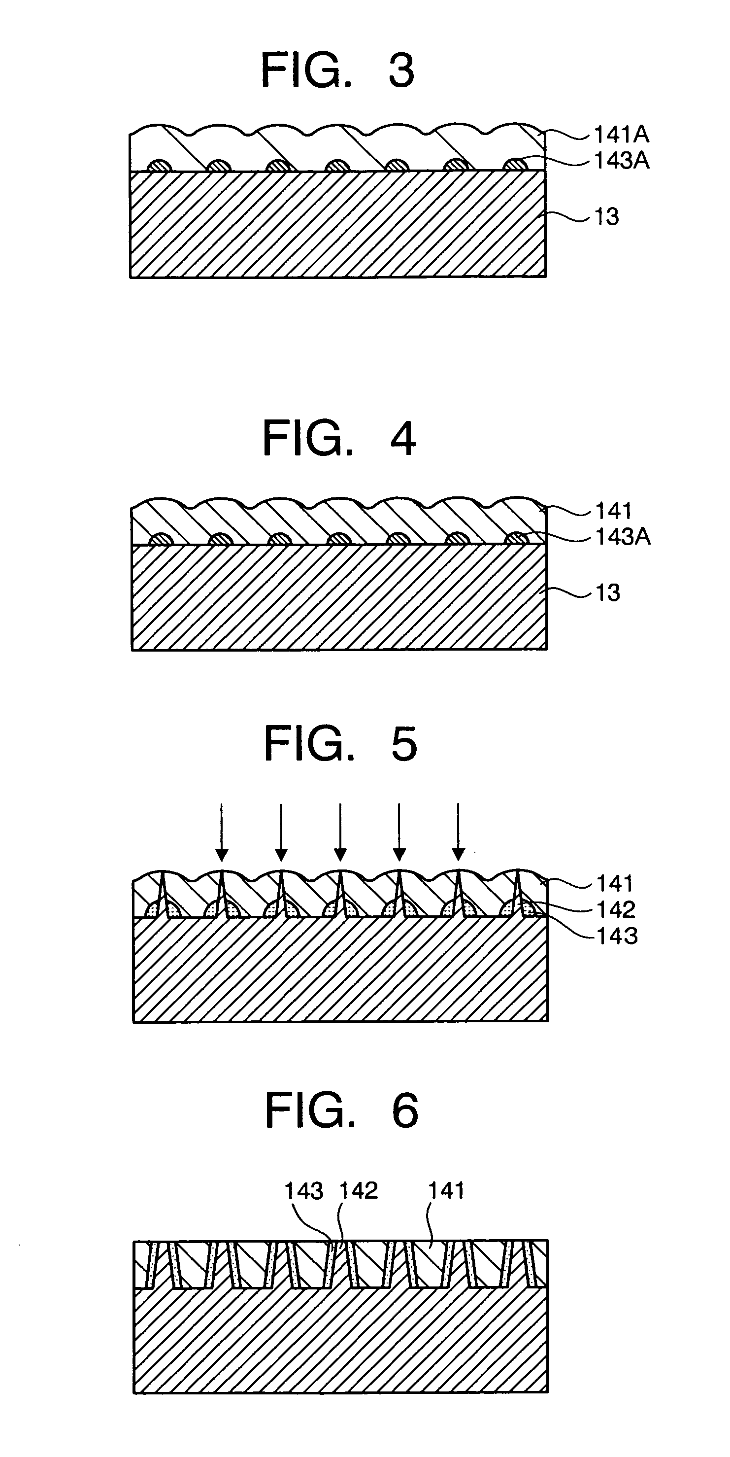
[0083]Metal to be compound layer: Ta 0.02 nm
[0084]Metal to be insulating layer: Al 0.9 nm (an Al layer is formed, naturally oxidized and heated)
[0085]Free layer 15: Fe5CO5 2.5 nm
[0086]Protective layer 16: Cu 1 nm / Ta 2 nm / Ru 15 nm
[0087]The thus obtained magneto-resistance effect element 10 was thermally treated at 270° C. during 10 hours under magnetic field. The variation ratio in resistance of the magneto-resistance effect element 10 in Example 1 was larger than the variation ratio in resistance of a magneto-resistance effect element with no metal to be a compound layer. Moreover, the resistance ...
example 2
[0088]Example 2 relating to the magneto-resistance effect element 10 will be described. In Example 2, the magneto-resistance effect element 10 was formed as follows:
[0089]Underlayer 11: Ta 5 nm / Ru 2 nm Antiferromagnetic layer 12: PtMn 15 nm
[0090]First pinned layer 131: Co9Fe1 3.3 nm
[0091]Antiparallel-magnetic coupling layer 132: Ru 0.9 nm
[0092]Second pinned layer 132: Fe5CO5 2.5 nm
[0093]Metal to be compound layer: Ta 0.02 nm
[0094]Metal to be insulating layer: Al 0.9 nm (an Al layer is formed, naturally oxidized and heated)
[0095]Free layer 15: Fe5CO5 2.5 nm
[0096]Protective layer 16: Cu 1 nm / Ta 2 nm / Ru 15 nm
[0097]The thus obtained magneto-resistance effect element 10 was thermally treated at 270° C. during 10 hours under magnetic field. The variation ratio in resistance of the magneto-resistance effect element 10 in Example 2 was larger than the variation ratio in resistance of a magneto-resistance effect element with no metal to be a compound layer. Moreover, the resistance of the ma...
example 3
[0098]Example 3 relating to the magneto-resistance effect element 10 will be described. In Example 3, the magneto-resistance effect element 10 was formed as follows:
[0099]Underlayer 11: Ta 5 nm / Ru 2 nm
[0100]Antiferromagnetic layer 12: IrMn 10 nm
[0101]First pinned layer 131: Co9Fe1 3.3 nm
[0102]Antiparallel-magnetic coupling layer 132: Ru 0.9 nm
[0103]Second pinned layer 132: Fe5CO5 2.5 nm
[0104]Metal to be compound layer: Ta 0.02 nm
[0105]Metal to be insulating layer: Al2O3 1.2 nm (an Al2O3 layer is formed and heated)
[0106]Free layer 15: Fe5CO5 2.5 nm
[0107]Protective layer 16: Cu 1 nm / Ta 2 nm / Ru 15 nm
[0108]The thus obtained magneto-resistance effect element 10 was thermally treated at 270° C. during 10 hours under magnetic field. The variation ratio in resistance of the magneto-resistance effect element 10 in Example 3 was larger than the variation ratio in resistance of a magneto-resistance effect element with no metal to be a compound layer. Moreover, the resistance of the magneto-res...
PUM
| Property | Measurement | Unit |
|---|---|---|
| magneto-resistance | aaaaa | aaaaa |
| magnetization | aaaaa | aaaaa |
| magnetic | aaaaa | aaaaa |
Abstract
Description
Claims
Application Information