

Method of Forming Thin Film, Thin Film Forming Apparatus, Program and Computer-Readable Information Recording Medium
a technology of thin film and forming apparatus, which is applied in the direction of coating, chemical vapor deposition coating, metallic material coating process, etc., can solve the problems of reduced film-forming rate, difficult to make it be adsorption onto the substrate, and reduced adsorption amount of gas onto the substrate surface, etc., to achieve enhanced adsorption rate of source gas
- Summary
- Abstract
- Description
- Claims
- Application Information
AI Technical Summary
Benefits of technology
Problems solved by technology
Method used
Image

Examples
Embodiment Construction
[0034]Hereinafter, an embodiment of the present invention will be described together with the drawings.
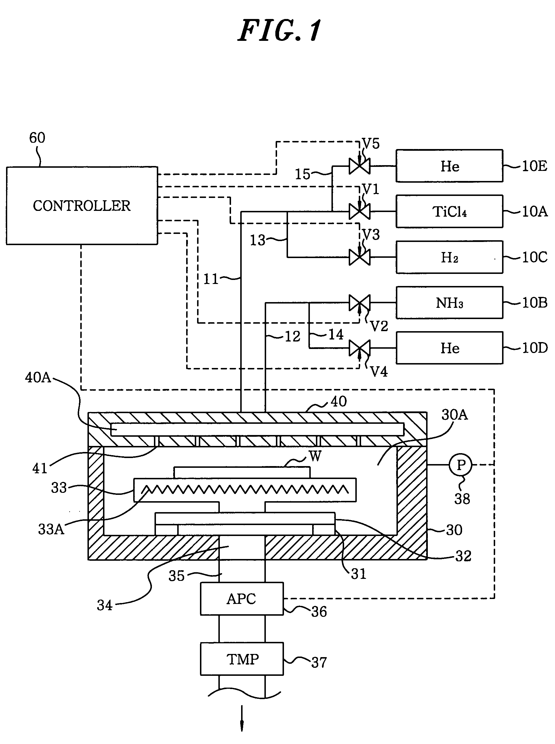
[0035]FIG. 1 shows a thin film forming apparatus in accordance with an embodiment of the present invention. In this embodiment, a CVD apparatus is shown as an example of the thin film forming apparatus. As a whole, the thin film forming apparatus shown in FIG. 1 includes gas supply sources 10A-10E, a processing chamber 30, a susceptor 33, and a controller 60.
[0036]The gas supply sources 10A-10E provide source gases described later and the like into the processing chamber 30 via gas passages 11-15. That is, the gas supply sources 10A-10E respectively provide a semiconductor wafer W in the processing chamber 30 with gases for performing a predetermined film forming process.
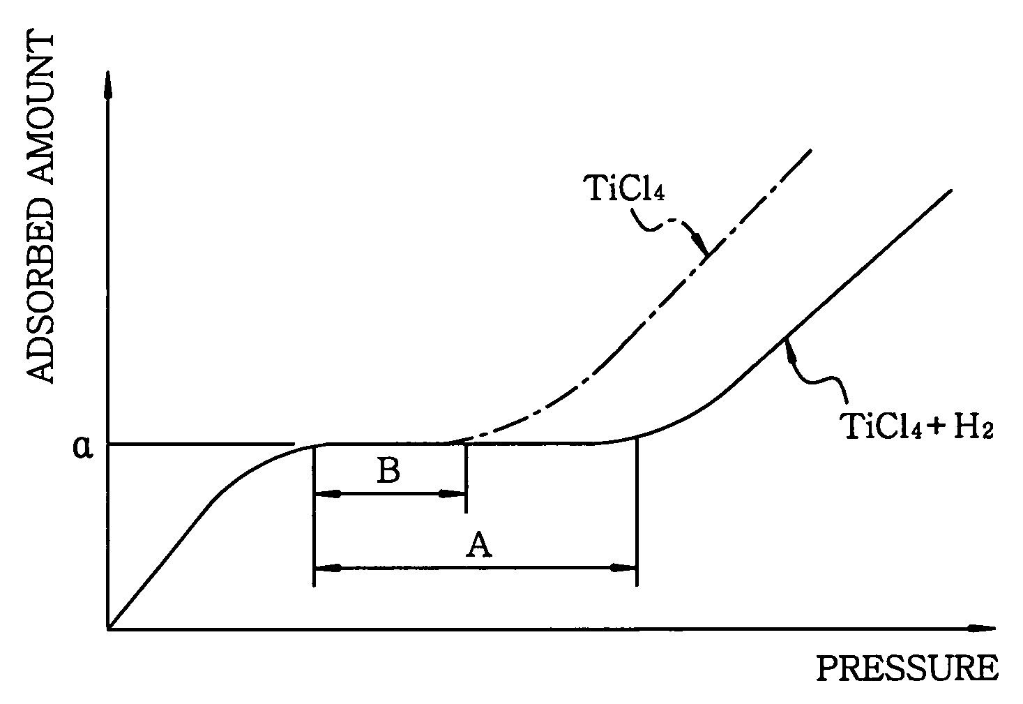
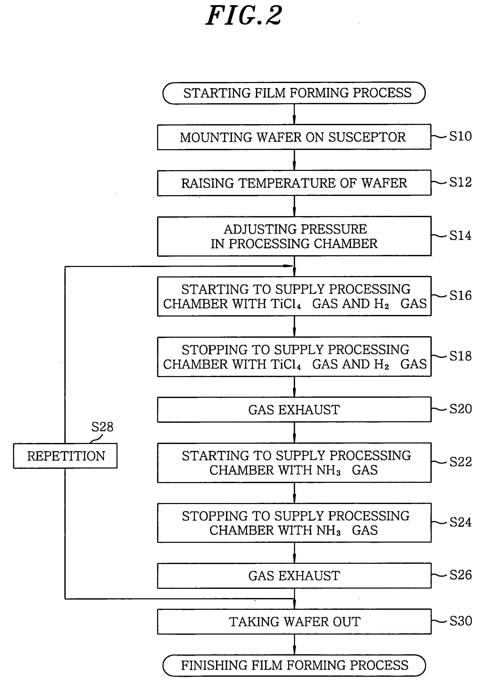
[0037]The thin film forming apparatus in accordance with the embodiment forms a titan nitride (TiN) film by using a chemical vapor deposition method. To be more specific, in this embodiment, a TiN film is formed by...
PUM
| Property | Measurement | Unit |
|---|---|---|
| temperature | aaaaa | aaaaa |
| temperature | aaaaa | aaaaa |
| pressure | aaaaa | aaaaa |
Abstract
Description
Claims
Application Information