Shallow trench isolation (STI) based laterally diffused metal oxide semiconductor (LDMOS)

a metal oxide semiconductor and laterally diffused technology, applied in the field of semiconductor devices, can solve the problems of reducing the lifetime of the transistor, affecting the efficiency of the transistor, and eventually destroying the transistor,

Inactive Publication Date: 2008-10-09
AVAGO TECH WIRELESS IP SINGAPORE PTE
View PDF81 Cites 45 Cited by
  • Summary
  • Abstract
  • Description
  • Claims
  • Application Information

AI Technical Summary

Problems solved by technology

As the operating voltage applied to a transistor increases, the transistor will eventually breakdown allowing an uncontrollable increase in current to pass through the junction.
Operating above the breakd...

Method used


Image

  • Shallow trench isolation (STI) based laterally diffused metal oxide semiconductor (LDMOS)
  • Shallow trench isolation (STI) based laterally diffused metal oxide semiconductor (LDMOS)
  • Shallow trench isolation (STI) based laterally diffused metal oxide semiconductor (LDMOS)

Examples


Embodiment Construction

[0021]The following detailed description of the present invention refers to the accompanying drawings that illustrate exemplary embodiments consistent with this invention. Other embodiments are possible, and modifications may be made to the embodiments within the spirit and scope of the invention. Therefore, the detailed description is not meant to limit the invention. Rather, the scope of the invention is defined by the appended claims.

[0022]References in the specification to “one embodiment,”“an embodiment,”“an example embodiment,” etc., indicate that the embodiment described may include a particular feature, structure, or characteristic, but every embodiment may not necessarily include the particular feature, structure, or characteristic. Moreover, such phrases are not necessarily referring to the same embodiment. Further, when a particular feature, structure, or characteristic is described in connection with an embodiment, it is submitted that it is within the knowledge of one s...


PUM


Abstract

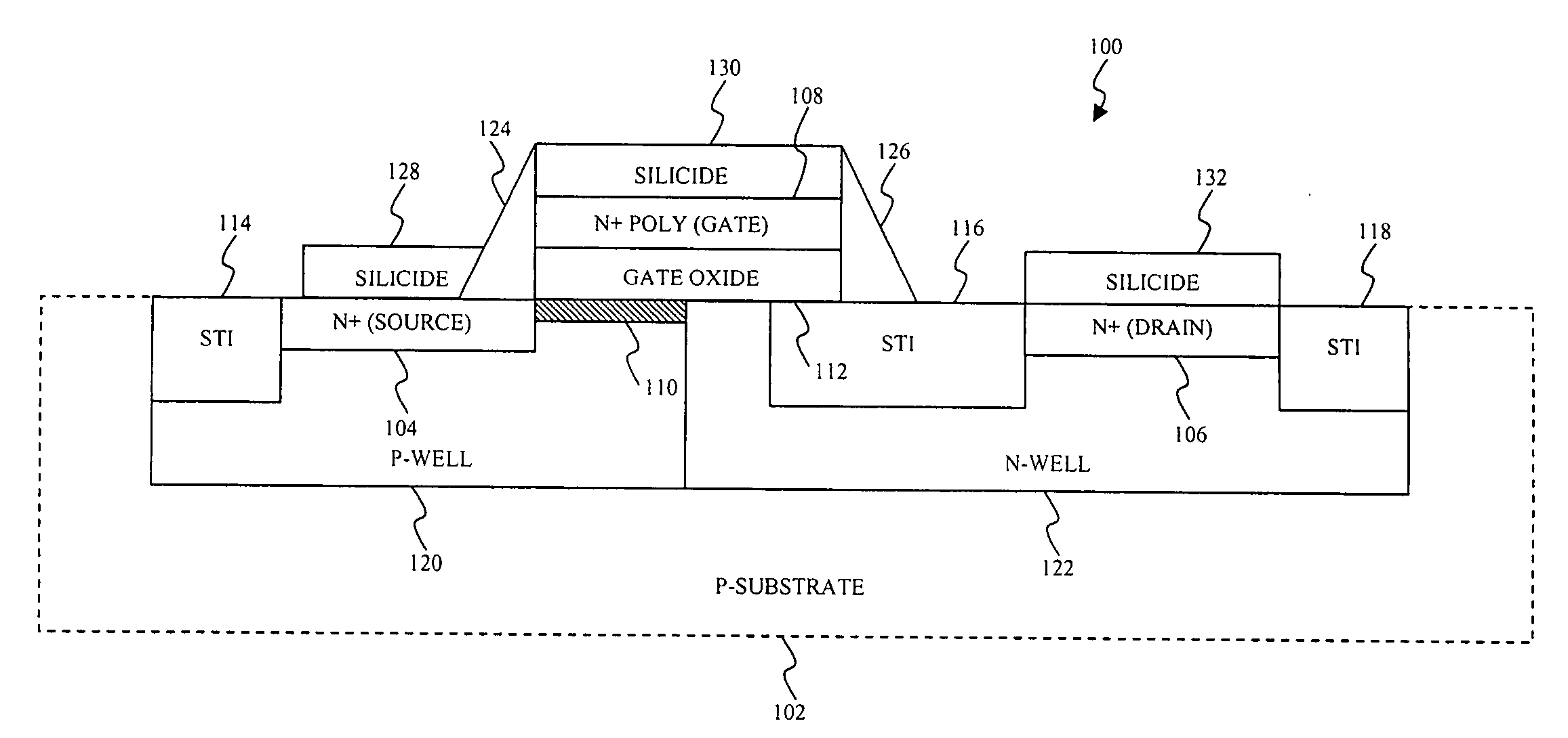
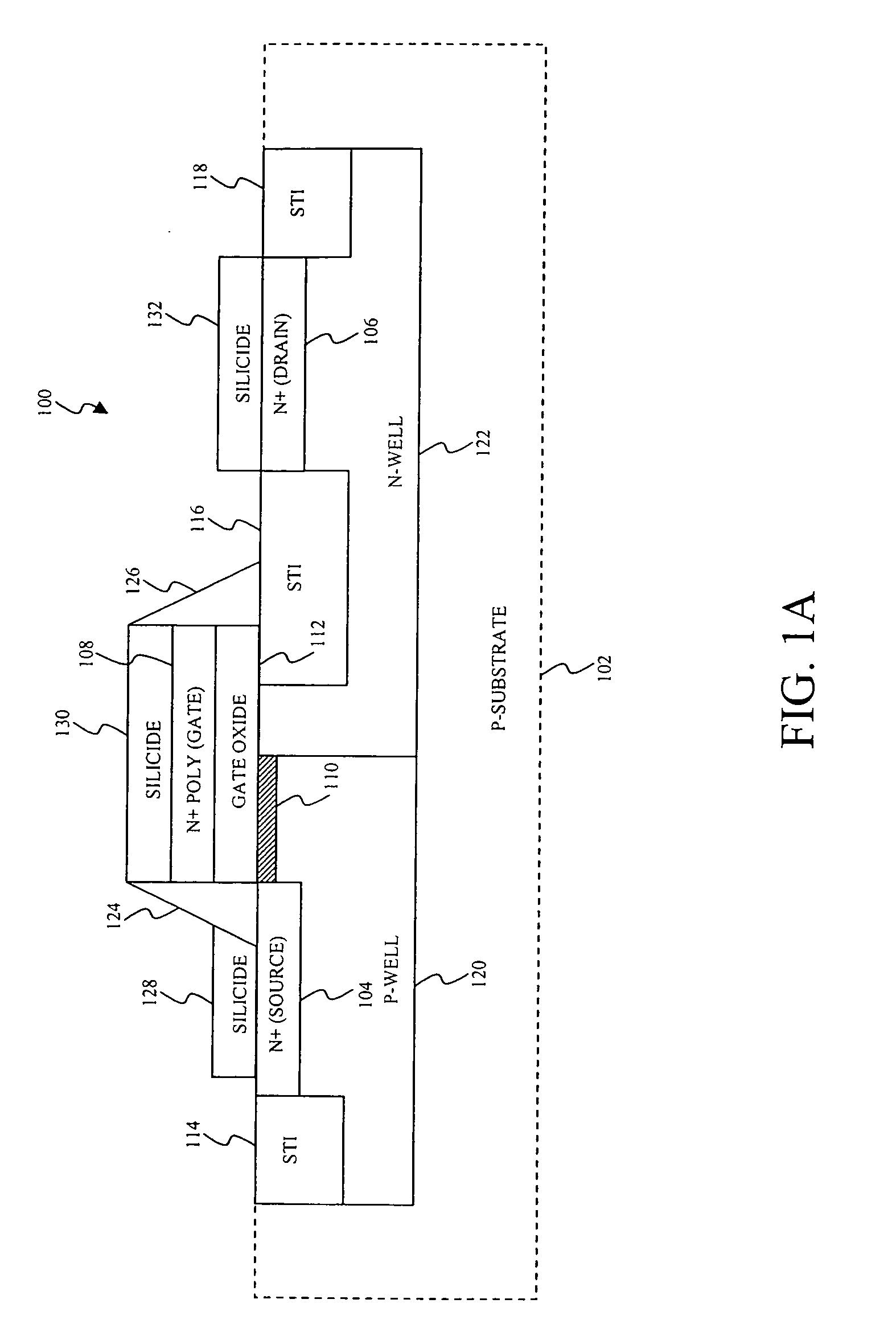
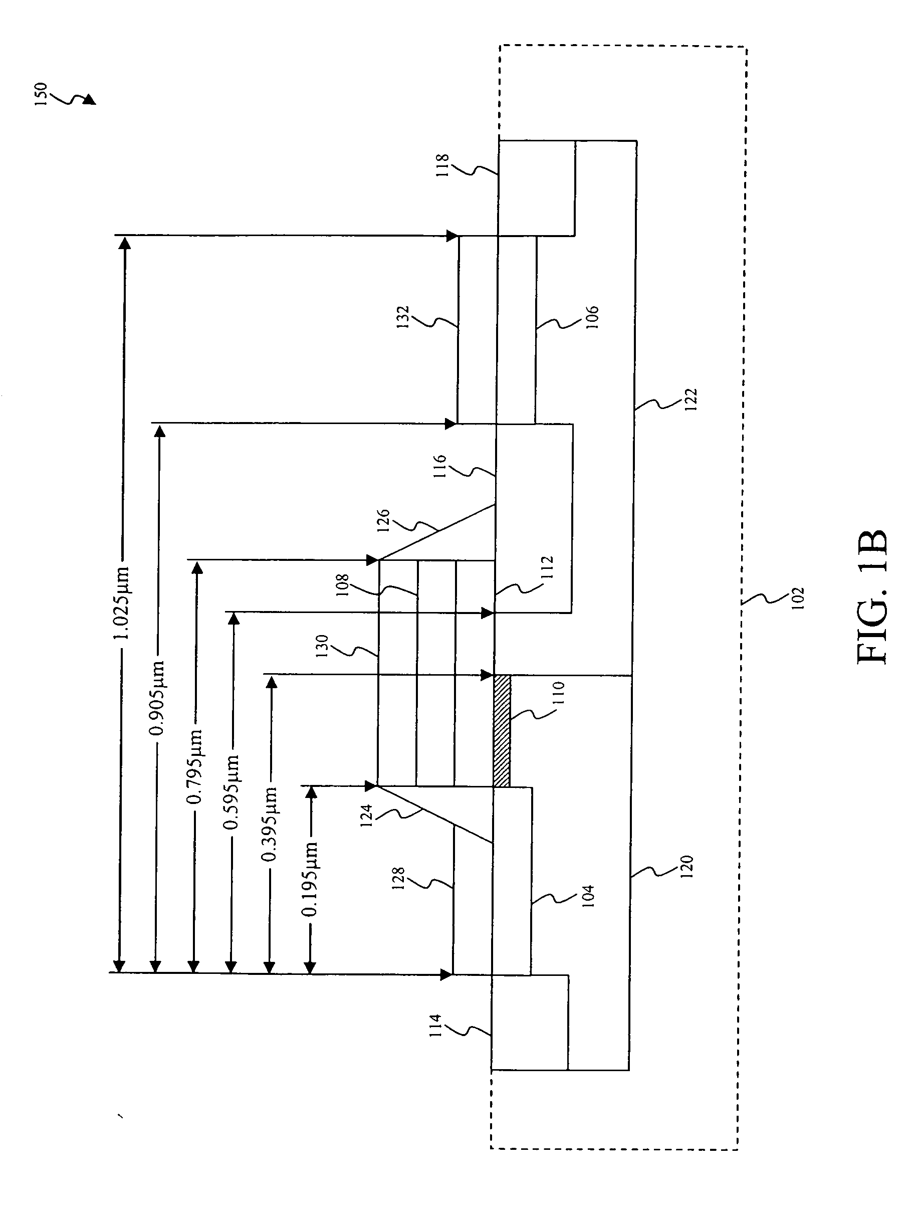
An apparatus is disclosed to increase a breakdown voltage of a semiconductor device. The semiconductor device includes a first heavily doped region to represent a source region. A second heavily doped region represents a drain region of the semiconductor device. A third heavily doped region represents a gate region of the semiconductor device. The semiconductor device further includes a shallow trench isolation (STI) region to increase the resistance from the drain region to the source region. The STI region includes a first side vertically aligned with a second side of the gate region. The STI region extends from the first side to a second side in contact with a second side of the drain region. The breakdown voltage of the n-type semiconductor device is directly proportional to a vertical length, or a depth, of the first side and/or the second side of the STI region. The horizontal length, or distance from the first side to the second side, of the STI region does not substantially contribute to the breakdown voltage of the semiconductor device. As a result, a conventional CMOS logic foundry technology may fabricate the STI region of the semiconductor device using a low operating voltage process minimum design rule.

Description

CROSS REFERENCE TO RELATED APPLICATIONS[0001]This application is a continuation in part of U.S. patent application Ser. No. 11 / 580,961, filed Oct. 16, 2006 which claims benefit of U.S. Provisional Application No. 60 / 833,787, filed Jul. 28, 2006, all of which are incorporated herein by reference in their entirety.FIELD OF THE INVENTION[0002]The present invention generally relates to semiconductors. More specifically, the invention relates to increasing a breakdown voltage of a semiconductor device.BACKGROUND OF THE INVENTION[0003]Silicon semiconductor processing has evolved sophisticated operations for fabricating integrated circuits. As advancement in fabrication process technology continues, the operating voltage of the integrated circuits has decreased, but the operating voltage of auxiliary devices remains the same. Auxiliary devices are devices used in conjunction with integrated circuits and may include printers, scanners, disk drives, tape drives, microphones, speakers, and ca...

Claims


Application Information

Patent Timeline
IPC IPC(8): H01L29/78
CPCH01L29/0653H01L29/086H01L29/0865H01L29/1083H01L29/456H01L29/66659H01L29/7835
Inventor ITO, AKIRACHEN, HENRY KUO-SHUN
Owner AVAGO TECH WIRELESS IP SINGAPORE PTE
Why Eureka
Try Eureka