Solid state imaging device and fabrication method of solid state imaging device

a technology of solid-state imaging and fabrication method, which is applied in the direction of semiconductor/solid-state device manufacturing, semiconductor devices, electrical devices, etc., can solve the problems of deterioration and degeneration caused, the inability to avoid problems, and the inability to prevent deterioration. , to achieve the effect of preventing deterioration

Active Publication Date: 2008-10-09
FUJIFILM CORP
View PDF3 Cites 38 Cited by
  • Summary
  • Abstract
  • Description
  • Claims
  • Application Information

AI Technical Summary

Benefits of technology

[0007]The invention has been made in consideration of the aforementioned situation, in a solid state imaging device including a pair of electrodes and a photoelectric conversion film interposed

Problems solved by technology

Thus, there is concern about occurrence of deterioration and degeneration caused by the ozone in the upper electrodes and the photoelectric conversion film.
As described in WO0

Method used


Image

  • Solid state imaging device and fabrication method of solid state imaging device
  • Solid state imaging device and fabrication method of solid state imaging device
  • Solid state imaging device and fabrication method of solid state imaging device

Examples


Embodiment Construction

[0031]Hereinafter, an embodiment of the invention will be described with reference to the drawings.

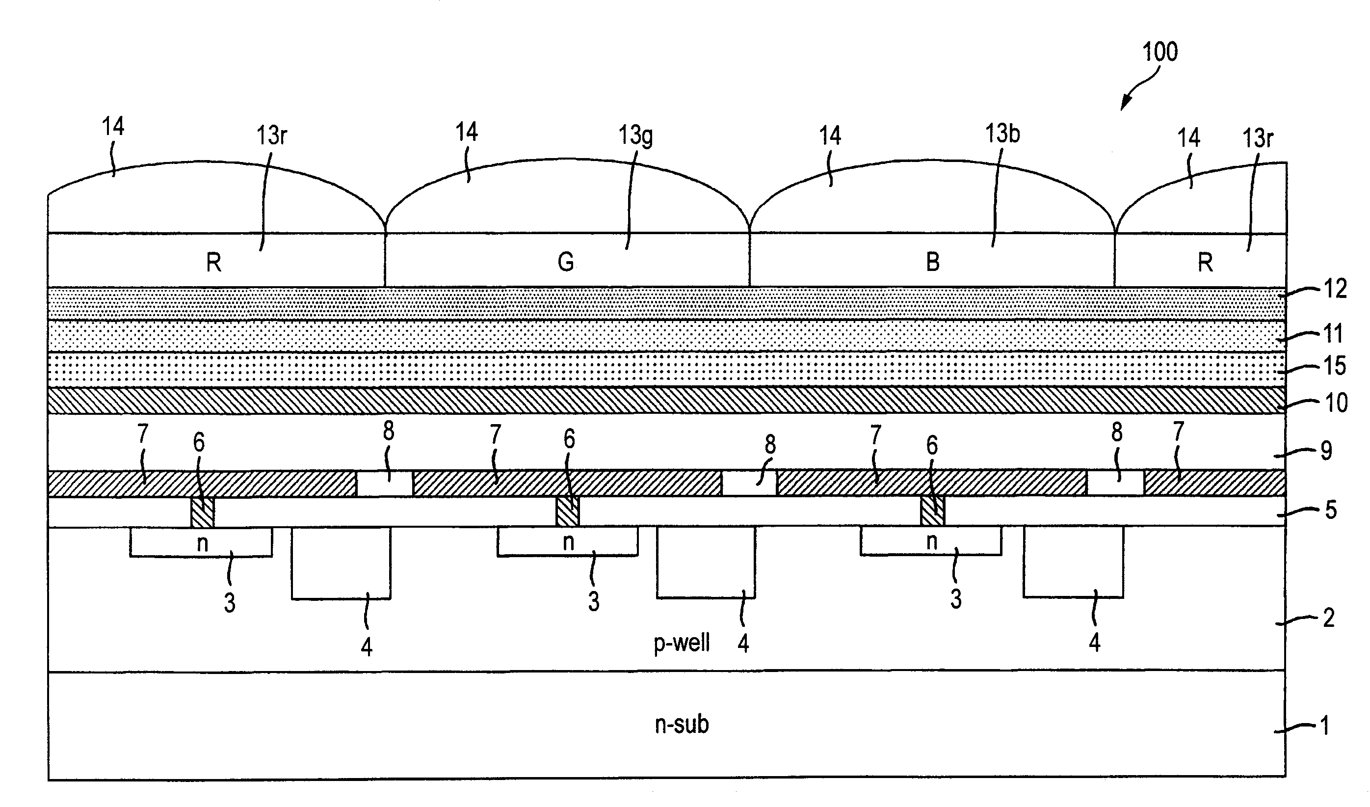
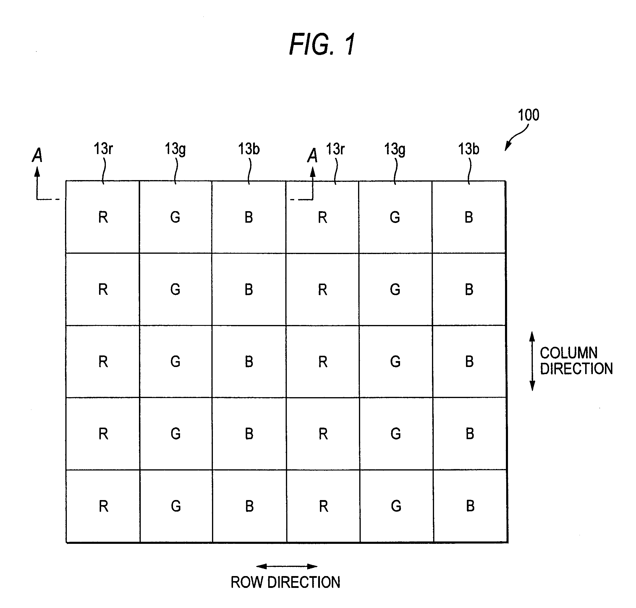
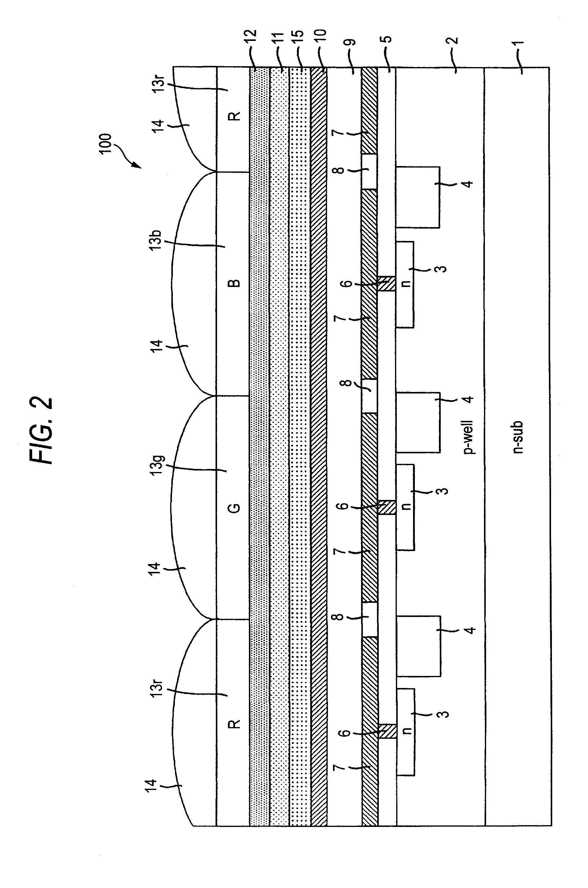
[0032]FIG. 1 is a schematic view illustrating a partial surface of a solid state imaging device 100 according to an embodiment of the invention. FIG. 2 is a sectional schematic view illustrating the solid state imaging device taken along line A-A shown in FIG. 1. In addition, in FIG. 1, a micro lens 14 is omitted.

[0033]On an n-type Si substrate 1, a p-well layer 2 is formed. Hereinafter, the n-type silicon substrate 1 and the p-well layer 2 together are referred to as a semiconductor substrate. In addition, the p-type Si substrate may be used as the semiconductor substrate. In a row direction on the identical surface of the upper side of the semiconductor substrate and a column direction orthogonal thereto, there are arranged a lot of color filters. There are three types of color filters including color filters 13r that mainly transmit light in an R wavelength region, color filters 13g...


PUM


Abstract

A solid state imaging device comprises: photoelectric conversion portions on or above a substrate; and color filters on or above the respective photoelectric conversion portions. Each of the photoelectric conversion portions comprises: a lower electrode on or above the substrate; a photoelectric conversion film on or above the lower electrode; and an upper electrode on or above the photoelectric conversion film. The device further comprises: a first inorganic material film that protects each of the photoelectric conversion portions, is formed by a first method and is above the upper electrode and below the color filters; a second inorganic material film that prevents characteristic deterioration of the photoelectric conversion portion caused by the first method, is formed by a second method and is between the upper electrode and the first inorganic material film; and a polymeric material film that enhances a function of the first inorganic material film and is on or above the first inorganic material film.

Description

BACKGROUND OF THE INVENTION[0001]1. Field of the Invention[0002]The present invention relates to a solid state imaging device having a plurality of photoelectric conversion portions arranged above a substrate and color filters formed above the plurality of photoelectric conversion portions, respectively.[0003]2. Description of the Related Art[0004]In JP-T-2002-502120 (FIG. 5B), there is disclosed a solid state imaging device configured so that a lower electrode is formed on a Si substrate, a photoelectric conversion film is formed of an organic photoelectric conversion material on the lower electrode, upper electrodes divided for every pixel are formed on the photoelectric conversion film, and color filters divided for every pixel are formed on each of the upper electrodes. According to the solid state imaging device as mentioned above, it is possible to increase light receiving areas of pixels, and thus it is possible to increase sensitivity, as compared with a single plate type so...

Claims


Application Information

Patent Timeline
IPC IPC(8): H01L31/0232H01L31/18
CPCH01L27/1462H01L27/14621H01L27/14623H01L27/14627H01L27/14632H01L27/14645H01L27/14687
Inventor MAEHARA, YOSHIKI
Owner FUJIFILM CORP
Why Eureka
Try Eureka