Power Semiconductor Module for Inverter Circuit System

a technology of inverter circuit system and power semiconductor, which is applied in the direction of semiconductor devices, semiconductor device details, electrical apparatus, etc., can solve the problems of large amount of heat generated in the power semiconductor and long use period, so as to improve productivity and reliability, improve cooling efficiency, and increase productivity and reliability

Active Publication Date: 2008-10-16
HITACHI ASTEMO LTD
View PDF3 Cites 83 Cited by
  • Summary
  • Abstract
  • Description
  • Claims
  • Application Information

AI Technical Summary

Benefits of technology

[0013]It is an object of the present invention to improve cooling efficiency and in reliability of semiconductor module for use in converter circuit to be used in a power conversion device required when it is commercialized.
[0014]One of basic features of the present invention for solving the above-mentioned problem is that a semiconductor module incorporates therein a series circuit including an upper arm and a lower arm of an inverter circuit. The semiconductor module includes a heat dissipation member on each side thereof and a conducting member is fixed to one of the heat dissipation members through an insulating member. The series circuit is mounted on the conducting member. With this construction, most of works for forming the inverter circuit can be performed on one of the heat dissipation member side, so that productivity and reliability can be increased.
[0015]To increase the productivity and reliability required for commercialization as mentioned above, the semiconductor module according to one embodiment of the present invention as detailed hereinbelow is constructed as follows.

Problems solved by technology

When the switching action is performed, a large amount of heat is generated in the power semiconductor.
For this reason, it is an important problem to prevent this temperature increase.
In particular, the in-vehicle power conversion device to be mounted on an automobile is required to be accommodated in a relatively small space and despite this convert a large amount of power.
In spite of the fact that the power conversion device is used in a situation where vibration is always applied thereto, it is used for a long period of time.

Method used


Image

  • Power Semiconductor Module for Inverter Circuit System
  • Power Semiconductor Module for Inverter Circuit System
  • Power Semiconductor Module for Inverter Circuit System

Examples


Embodiment Construction

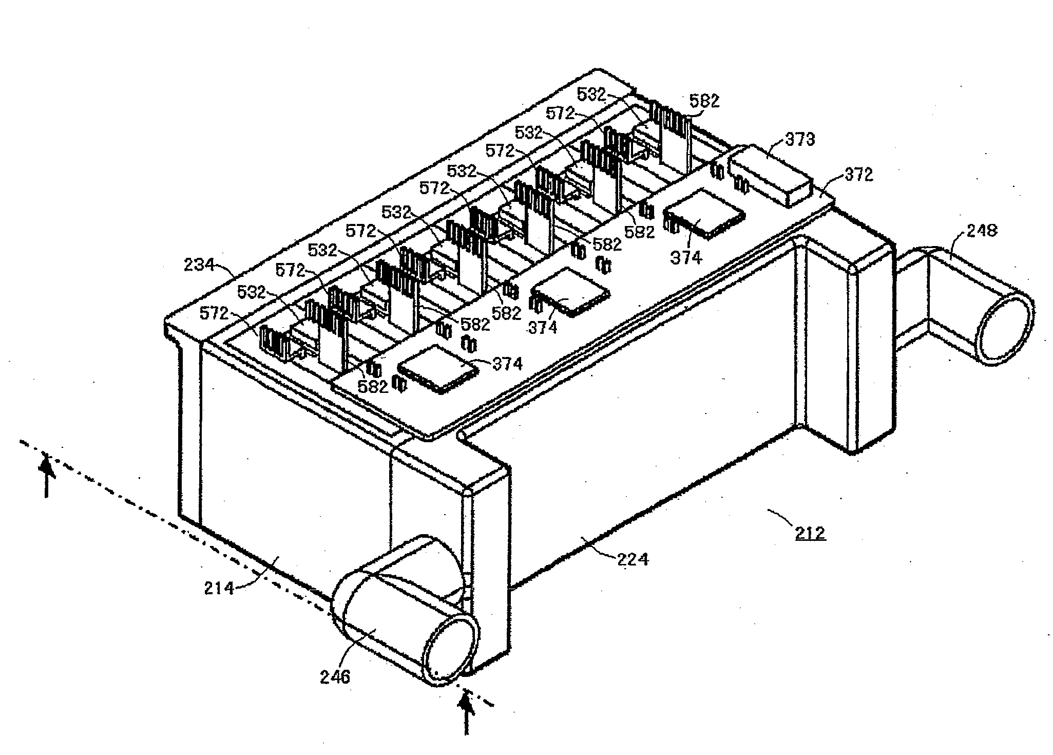
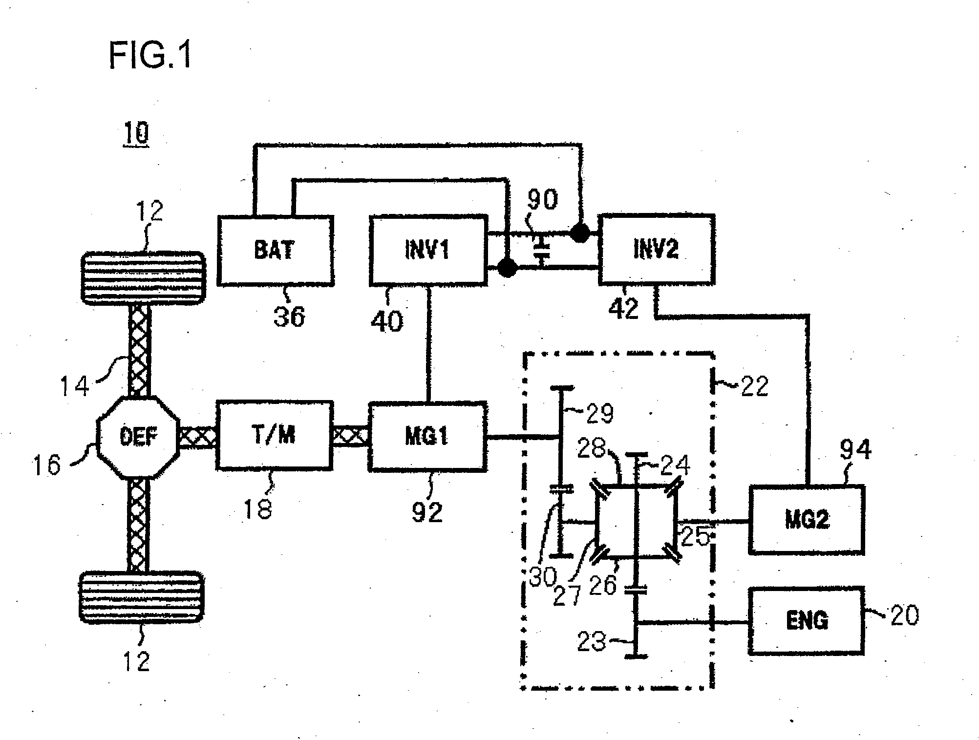
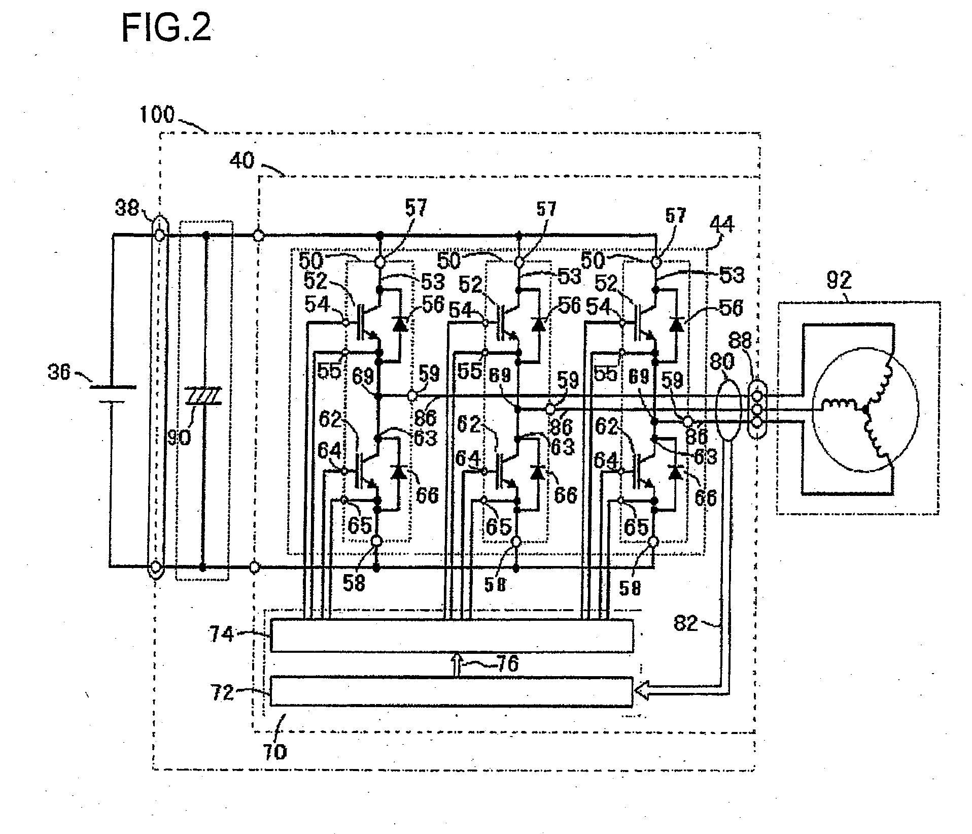
[0065]The following is a detailed description of the semiconductor module according to an embodiment of the present invention with reference to the attached drawings. First, technical problems on improvements and innovations on power conversion device according to an embodiment of the present invention and outline of the technology to solve the technical problems are described.

[0066]The power conversion device according to one embodiment of the present invention is made taking into consideration the following technical viewpoints so that they meet needs. One of the view points is a technology of downsizing, that is, a technology of preventing the size of power conversion device with an increasing power to be converted as much as possible. An other viewpoint is a technology relating to improvement of reliability of the power conversion device. Still another view point is a technology relating to improvement of productivity of the power conversion device. The power conversion device a...


PUM


Abstract

A double-face-cooled semiconductor module with an upper arm and a lower arm of an inverter circuit includes first and second heat dissipation members, each having a heat dissipation surface on one side and a conducting member formed on another side through an insulation member. On the conducting member on the first dissipation plate is provided with a fixing portion that fixes a collector surface of the semiconductor chip and a gate conductor connected to a gate terminal of the semiconductor module. The gate electrode terminal and the gate conductor are wire bonded. The conducting member on the second heat dissipation member is connected to an emitter surface of the semiconductor chip connected to the first heat dissipation member. The productivity and reliability are improved by most of formation operations for the upper and lower arms series circuit on one of the heat dissipation member.

Description

INCORPORATION BY REFERENCE[0001]The disclosure of the following priority application is herein incorporated by reference:[0002]Japanese Patent Application No. 2007-096536 filed Apr. 2, 2007.BACKGROUND OF THE INVENTION[0003]1. Field of the Invention[0004]The present invention relates to a power conversion device equipped with an inverter circuit and more particularly to a power semiconductor module for an inverter circuit system having a heat dissipation member.[0005]2. Description of Related Art[0006]Some types of conventional technology intended to increase heat dissipation efficiency of a semiconductor module by efficiently transferring heat from the semiconductor module include, for example, the cooling structure are disclosed in Japanese Laid-Open Patent Application No. 2005-175163. According to the description of Japanese Laid-Open Patent Application No. 2005-175163, a semiconductor module is inserted in a hole formed in a radiator for inserting a semiconductor module to allow ...

Claims


Application Information

Patent Timeline
Patent Type & Authority Applications(United States)
IPC IPC(8): H01L23/367
CPCH01L23/473H01L25/072H01L25/115H01L2924/13055H02M7/003H02M7/81H01L2224/73265H01L2924/13091H01L2924/30107H05K7/20927H01L2924/1305H01L2224/48091H01L2224/48472H01L2924/00014H01L2924/00
Inventor TOKUYAMA, TAKESHINAKATSU, KINYASAITO, RYUICHI
Owner HITACHI ASTEMO LTD
Why Eureka
Try Eureka