Analog processing circuit, analog integrated circuit device, image reading device, and image forming apparatus

an integrated circuit and analog technology, applied in the field of analog integrated circuit devices, can solve the problems of degrading image quality, affecting image quality, and difference between clamped voltage and reference voltage obtained from differential measurement, and unable to eliminate the effect of inherent fluctuation

Inactive Publication Date: 2008-10-16
RICOH KK
View PDF10 Cites 59 Cited by
  • Summary
  • Abstract
  • Description
  • Claims
  • Application Information

AI Technical Summary

Benefits of technology

[0011]It is an object of the present invention to at least

Problems solved by technology

However, there is a possibility that the reference voltage fluctuates due to the charge fluctuation (ripples) in a CCD driving signal that is used for driving the CCD line image sensor.
That results in vertical lines or waves in the image thereby degrading the image quality.
The cause of such a problem is that the clamped voltage and the reference voltage are essentially different types of voltages.
Thus, a diffe

Method used


Image

  • Analog processing circuit, analog integrated circuit device, image reading device, and image forming apparatus
  • Analog processing circuit, analog integrated circuit device, image reading device, and image forming apparatus
  • Analog processing circuit, analog integrated circuit device, image reading device, and image forming apparatus

Examples


Embodiment Construction

[0030]Exemplary embodiments of the present invention are described in detail below with reference to the accompanying drawings. The present invention is not limited to these exemplary embodiments.

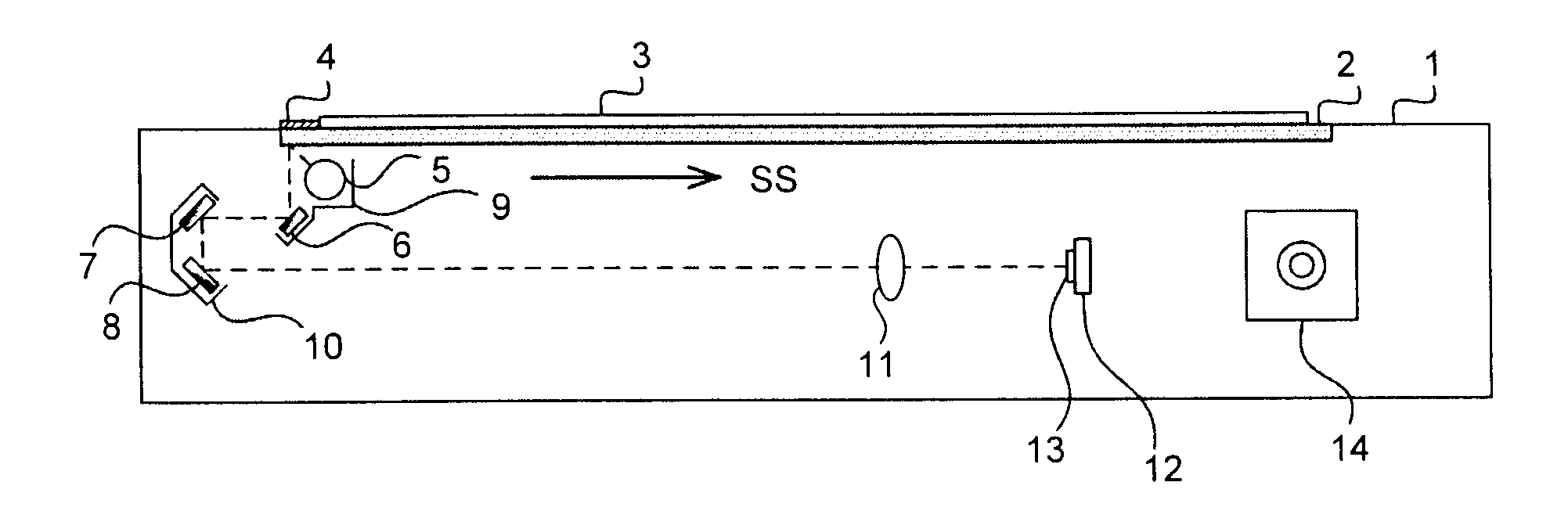
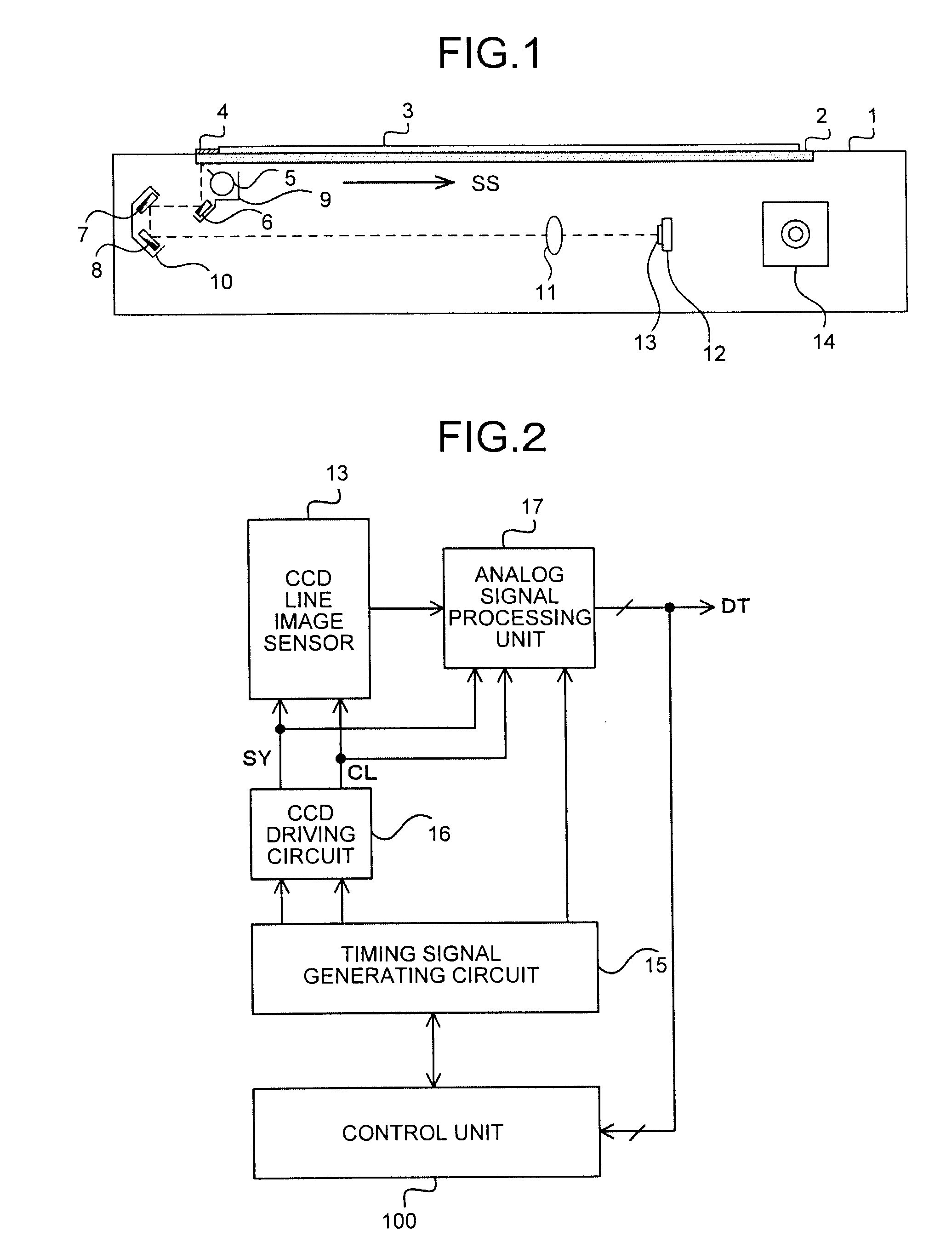
[0031]FIG. 1 is a schematic diagram of an image reading device according to a first embodiment of the present invention.

[0032]As shown in FIG. 1, a contact glass 2 is arranged on the upper surface of a housing 1 of the image reading device. An original document 3 having an image thereon is mounted between the contact glass 2 and a pressure plate (not shown). The pressure plate is arranged such that a target surface for reading of the original document 3 is maintained in close contact with the contact glass 2. A white standard board 4 is arranged at the left end of the contact glass 2, from where the image reading device starts reading the image on the original document 3. The white standard board 4 is used to obtain a white shading correction image.

[0033]After the target surface of the orig...


PUM


Abstract

A first clamping unit clamps a base voltage of an input image signal to a predetermined reference voltage. A sampling-and-holding unit samples and holds the image signal after clamping or a reference signal that becomes the base voltage of the image signal. An amplifying unit amplifies the image signal sampled and held by the sampling-and-holding unit. An analog-to-digital converting unit converts the image signal after amplification into a digital image signal. A second clamping unit clamps the reference signal to a predetermined voltage.

Description

CROSS-REFERENCE TO RELATED APPLICATIONS[0001]The present application claims priority to and incorporates by reference the entire contents of Japanese priority document 2007-107133 filed in Japan on Apr. 16, 2007.BACKGROUND OF THE INVENTION[0002]1. Field of the Invention[0003]The present invention relates to an analog processing circuit, an analog integrated circuit device, an image reading device, and an image forming apparatus.[0004]2. Description of the Related Art[0005]Generally, in an image reading device (e.g., a scanner) mounted on an image forming apparatus (e.g., a copying machine), a sheet having an image thereon is irradiated with a light and the light reflected from the sheet is converted into an analog image signal through a charged-coupled device (CCD) line image sensor such that the image on the sheet is read. Consequently, the analog image signal is subjected to a number of analog processes in an analog front end (AFE) that is an analog integrated circuit device. The ...

Claims


Application Information

Patent Timeline
IPC IPC(8): H03M1/12H04N5/14
CPCH03M1/0607H03M1/1295
Inventor NAKAZAWA, MASAMOTOKANNO, TOHRU
Owner RICOH KK
Why Eureka
Try Eureka