Resistive memory cell fabrication methods and devices

a technology of resistive memory and fabrication methods, which is applied in the direction of digital storage, semiconductor/solid-state device details, instruments, etc., can solve the problems of large power consumption, unsuitable portable devices or as substitutes for frequently-accessed volatile memory devices, and areas that are not as responsive to phase-changing currents

Active Publication Date: 2008-10-23
OVONYX MEMORY TECH LLC
View PDF33 Cites 22 Cited by
  • Summary
  • Abstract
  • Description
  • Claims
  • Application Information

AI Technical Summary

Problems solved by technology

Traditionally, however, non-volatile memory devices occupy a large amount of space and consume large quantities of power, making these devices unsuitable for use in portable devices or as substitutes for frequently-accessed volatile memory devices.
However, volatile memory devices require a continuous power supply in order to retain stored memory content.
Second, because certain areas of the GST material have a very low current density, these areas may not be as responsive to phase-changing currents.
It is even possible that regions near the lower electrode and lower edge may have insufficiently high current densities to fully transform the phase of the entire region of GST material near the lower electrode.
In other words, the application of a read voltage Vr could result in stray or leak currents through incompletely transformed regions of the GST material, thus resulting in erroneous GST phase state determination.

Method used


Image

  • Resistive memory cell fabrication methods and devices
  • Resistive memory cell fabrication methods and devices
  • Resistive memory cell fabrication methods and devices

Examples


Embodiment Construction

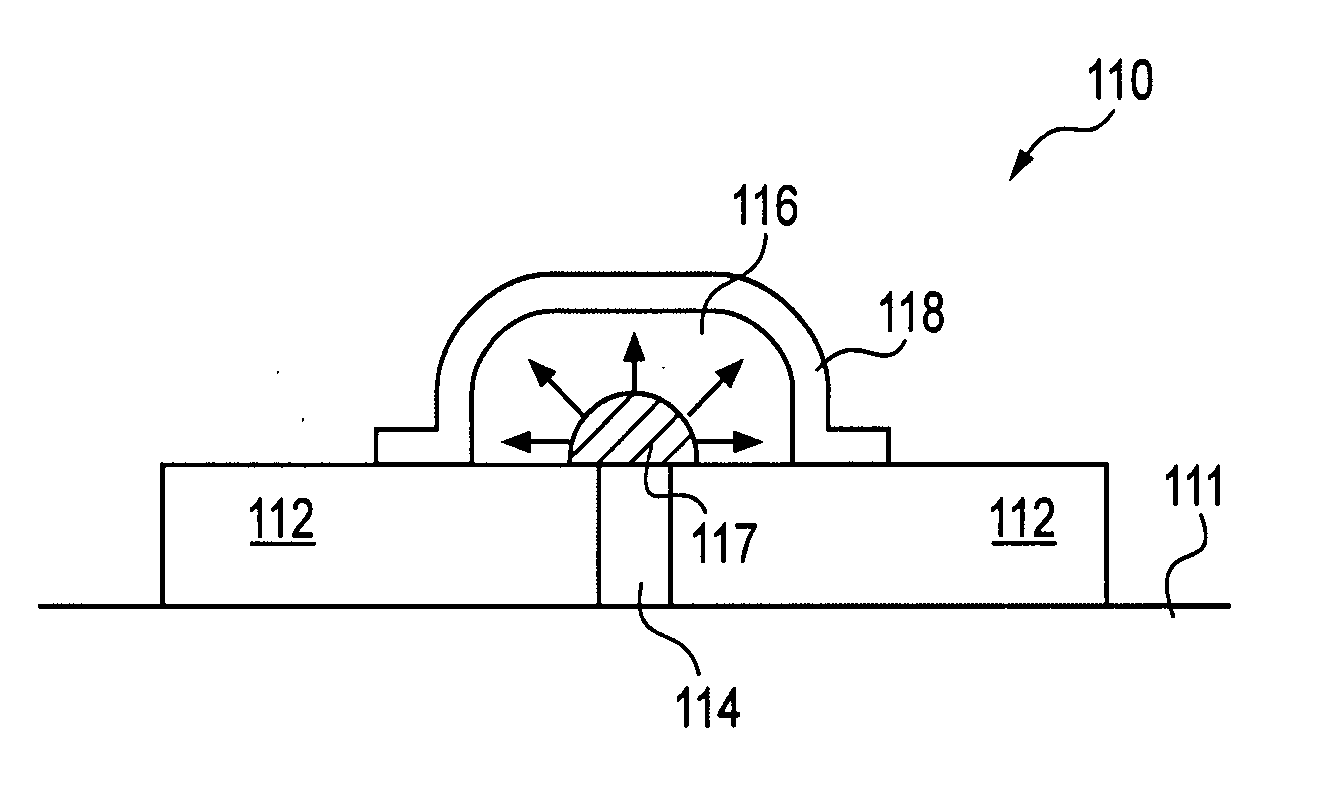
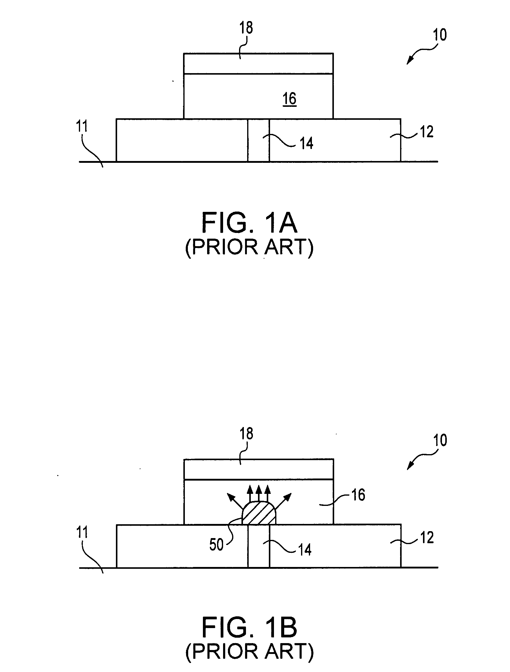
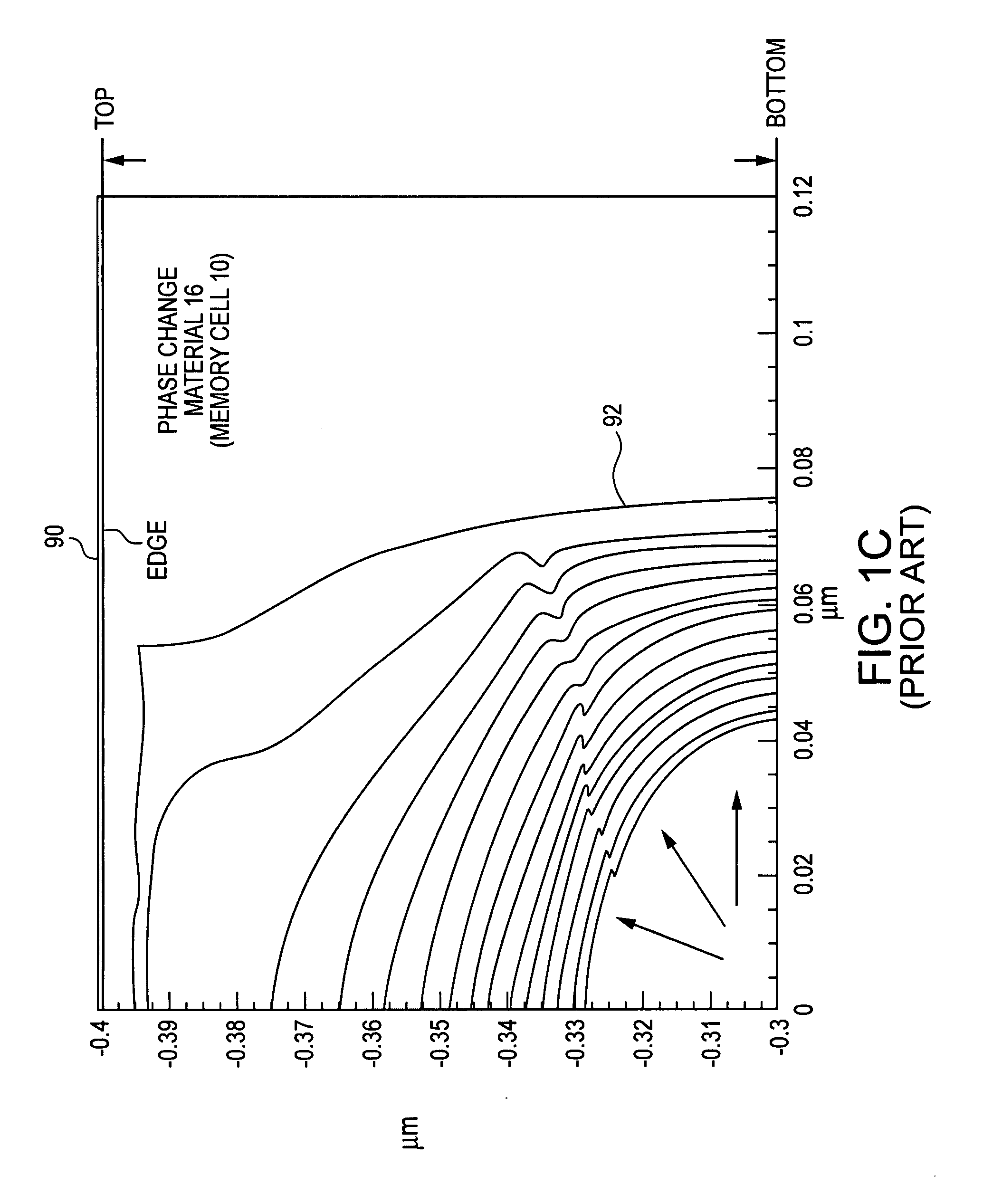
[0028]The term “substrate” used in the following description may include any supporting structure including, but not limited to, a semiconductor substrate that has an exposed substrate surface. A semiconductor substrate should be understood to include silicon, silicon-on-insulator (SOI), silicon-on-sapphire (SOS), doped and undoped semiconductors, epitaxial layers of silicon supported by a base semiconductor foundation, and other semiconductor structures, including those made of semiconductors other than silicon. When reference is made to a semiconductor substrate or wafer in the following description, previous process steps may have been utilized to form regions or junctions in or over the base semiconductor or foundation. The substrate also need not be semiconductor-based, but may be any support structure suitable for supporting an integrated circuit, including, but not limited to, metals, alloys, glasses, polymers, ceramics, and any other supportive materials as is known in the a...


PUM


Abstract

A phase change memory cell and methods of fabricating the same are presented. The memory cell includes a variable resistance region and a top and bottom electrode. The shapes of the variable resistance region and the top electrode are configured to evenly distribute a current with a generally hemispherical current density distribution around the first electrode.

Description

FIELD OF THE INVENTION[0001]The embodiments of the invention relate generally to the field of semiconductor devices and, more particularly, to resistive memory devices, for example, phase change memory devices.BACKGROUND OF THE INVENTION[0002]Microprocessor-accessible memory devices have traditionally been classified as either non-volatile or volatile memory devices. Non-volatile memory devices are capable of retaining stored information even when power to the memory device is turned off. Traditionally, however, non-volatile memory devices occupy a large amount of space and consume large quantities of power, making these devices unsuitable for use in portable devices or as substitutes for frequently-accessed volatile memory devices. On the other hand, volatile memory devices tend to provide greater storage capability and programming options than non-volatile memory devices. Volatile memory devices also generally consume less power than non-volatile devices. However, volatile memory ...

Claims


Application Information

Patent Timeline
Patent Type & Authority Applications(United States)
IPC IPC(8): H01L47/00H01L21/02
CPCG11C13/0004H01L27/2436H01L45/06H01L45/122H01L45/144H01L45/1675H01L45/1608H01L23/02H01L21/02H01L2924/0002H01L45/1683H01L2924/00H10B63/30H10N70/821H10N70/231H10N70/066H10N70/8828H10N70/063H10N70/021
Inventor LIU, JUNVIOLETTE, MIKE
Owner OVONYX MEMORY TECH LLC
Why Eureka
Try Eureka