Light emitting diode chip

a light-emitting diode and chip technology, applied in the direction of semiconductor/solid-state device manufacturing, electrical equipment, semiconductor devices, etc., can solve the problems of difficult etching of thick layers of gan-based materials, reducing the light output and operating life of leds, and relatively slow growth methods

Inactive Publication Date: 2008-10-23
GOLDENEYE
View PDF6 Cites 87 Cited by
  • Summary
  • Abstract
  • Description
  • Claims
  • Application Information

AI Technical Summary

Benefits of technology

[0015]In one embodiment of this invention, an assembly for a thick substrate free light emitting diode chip includes a multilayer semiconductor structure on a growth substrate. The multilayer semiconductor structure includes a first doped layer proximal to the growth substrate, an active region, and a second doped layer distal from the growth substrate with an active region interposed between the first doped layer and the second doped layer. The multilayer semiconductor structure is preferably at least 10 microns thick, but can be 30 microns or more thick

Problems solved by technology

These growth methods are relatively slow and expensive.
Thick layers of GaN-based materials are, however, difficult to etch, especially anisotropically.
The heat lowers the light output and operating lifetime of the LED.
As LED sizes become larger, such heating effects become more important and can seriously degrade the light-output performance and lifetime of the LEDs.
Sapphire is a poor thermal conductor.
Cheung et al. do not disclose using a raster-scanned pulsed laser beam to both separate the semiconductor layer from the substrate and to simultaneously form surface features that can be used as light extraction elements in LED devices fabricated from the semiconductor layer.
Cheung et al. also do not disclose methods to etc

Method used


Image

  • Light emitting diode chip
  • Light emitting diode chip
  • Light emitting diode chip

Examples


Embodiment Construction

[0047]The preferred embodiments of the present invention will be better understood by those skilled in the art by reference to the above listed figures. The preferred embodiments of this invention illustrated in the figures are not intended to be exhaustive or to limit the invention to the precise form disclosed. The figures are chosen to describe or to best explain the principles of the invention and its applicable and practical use to thereby enable others skilled in the art to best utilize the invention.

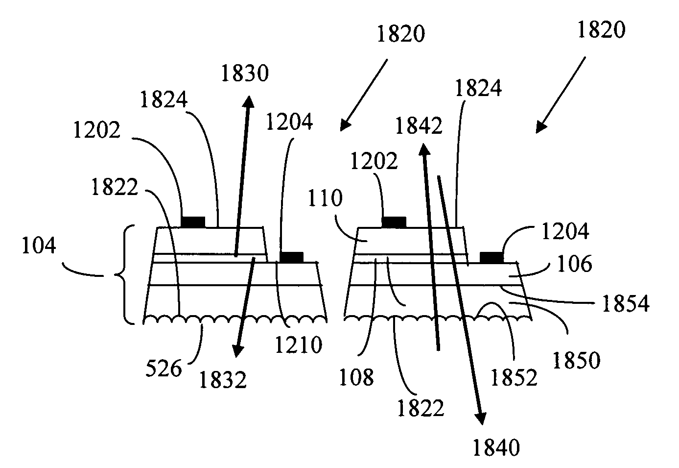
[0048]A thick LED semiconductor structure chip is at least 10 microns thick and does not need the original growth substrate or an attached transfer substrate for structural support.

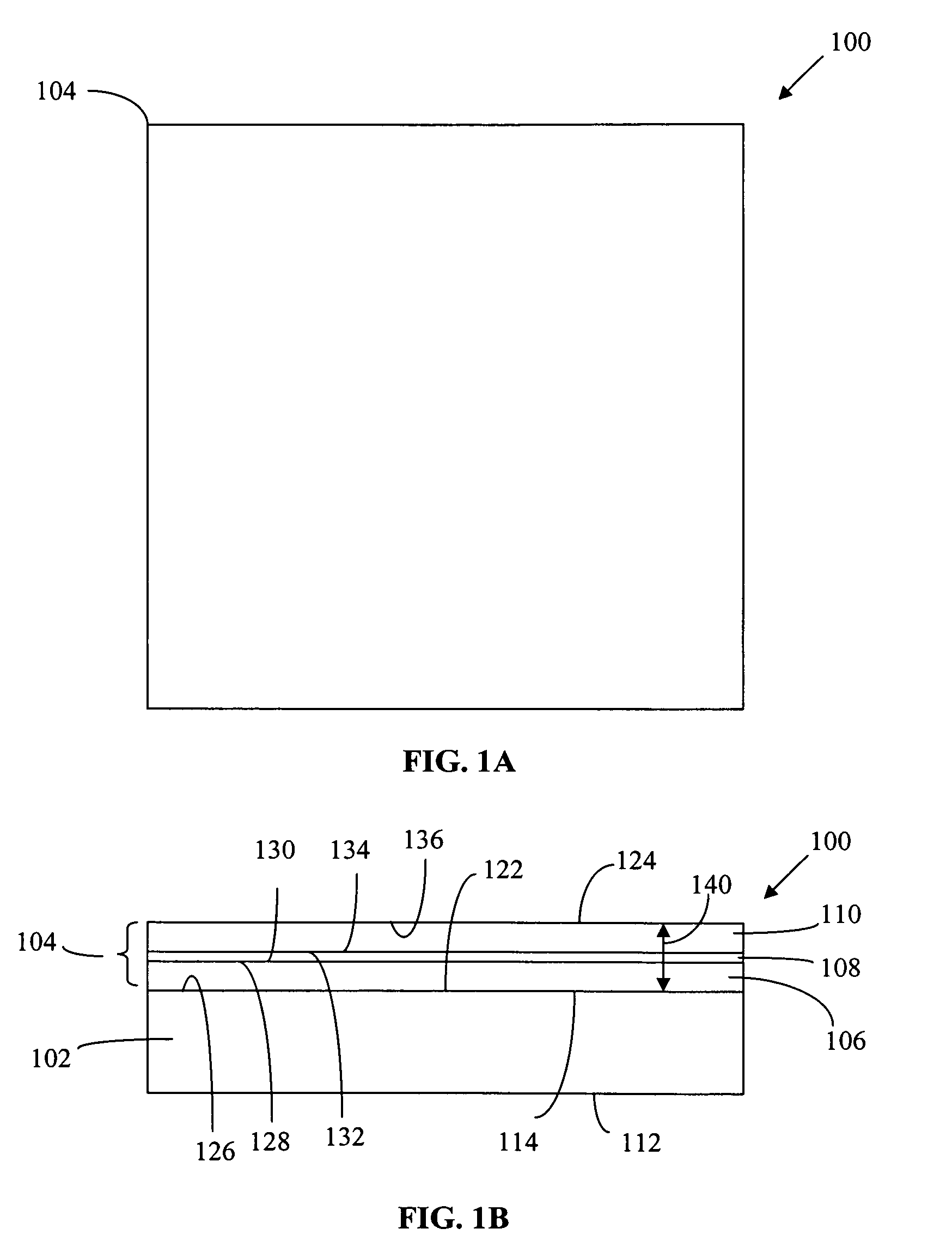
[0049]The first step to form a thick LED chip is to provide an assembly that includes a multilayer semiconductor structure on an optically transparent growth substrate. FIGS. 1A and 1B illustrate assembly 100 that includes a growth substrate 102 and a multilayer semiconductor structure 104. FIG. 1A is a...


PUM


Abstract

A substrate-free LED chip has a multilayer semiconductor structure at least 10 microns thick provided on a growth substrate. One or more arrays of parallel streets are etched into the multilayer semiconductor structure using a first pulsed laser beam. By scanning a second pulsed laser beam through the growth substrate to the multilayer semiconductor structure, the LED chips are detached from the growth substrate while simultaneously forming surface features on the chips.

Description

REFERENCE TO PRIOR APPLICATION[0001]This application claims the benefit of U.S. Provisional Patent Application Ser. No. 60 / 925,961, filed on Apr. 23, 2007, which is herein incorporated by reference.TECHNICAL FIELD[0002]The present invention is a thick light emitting diode chip, is substrate-free and requires no growth substrate or transfer substrate for structural support.BACKGROUND OF THE INVENTION[0003]Light emitting diodes (LEDs) can be fabricated by epitaxially growing multiple layers of semiconductors on a growth substrate. Inorganic light-emitting diodes can be fabricated from GaN-based semiconductor materials containing gallium nitride (GaN), aluminum nitride (AlN), aluminum gallium nitride (AlGaN), indium nitride (InN), indium gallium nitride (InGaN) and aluminum indium gallium nitride (AlInGaN). Other appropriate materials for LEDs include, for example, aluminum gallium indium phosphide (AlGaInP), gallium arsenide (GaAs), indium gallium arsenide (InGaAs), indium gallium ars...

Claims


Application Information

Patent Timeline
IPC IPC(8): H01L33/00H01L21/00H01L33/22
CPCH01L33/0079H01L33/0095H01L33/22H01L33/0093
Inventor ZIMMERMAN, SCOTT M.BEESON, KARL W.LIVESAY, WILLIAM R.
Owner GOLDENEYE
Why Eureka
Try Eureka