Transparent conductive laminate and touch panel therewith

Active Publication Date: 2008-10-23
NITTO DENKO CORP
View PDF7 Cites 21 Cited by
  • Summary
  • Abstract
  • Description
  • Claims
  • Application Information

AI Technical Summary

Benefits of technology

[0024]According to the invention, a two-layer structure of transparent conductive thin film is formed on a transparent film substrate, similarly to Patent Literature 3, and such a two-layer structure comprises a first transparent conductive thin film of an indium-tin complex oxide with a relatively low SnO2 content formed on the film substrate and a second transparent conductive thin film of an indium-tin complex oxide with a relatively high SnO2 content formed on the first transparent conductive thin film. However, the SnO2 content of each of the first and second transparent conductive thin films is limited within a relatively low range, as compared with that in Patent Literature 3. In addition, the thickness of each of the first and second transparent conductive thin films and the sum of the thicknesses of both thin films are each set in a specific range. According to the invention, the SnO2 content of each of the first and second transparent conductive thin films and the thickness of each thin film are controlled as described above so that these thin films can be sufficiently crystallized by a heat treatment at a low temperature of 150° C. or less, which is acceptable to the film substrate, and thus the transparent conductive thin films can be provided with a crystalline film structure. According to the invention, therefore, the crystalline structure of the transparent conductive thin films can provide satisfactory surface pressure durability in addition to transparency and pen input durability and also allows the production of transparent conductive thin films with high reliability at high temperature and high humidity.
[0025]According to the invention, the structure of the transparent conductive laminate includes a transparent laminated base substrate that is provided on the transparent condu

Problems solved by technology

Since the conductive glass has a glass substrate, however, it has low flexibility or workability, and cannot be used for certain purposes in some cases.
However, such conventional transparent conductive films not only have the problem of low transparency due to high light reflectance of the thin film surface but also have low scratch resistance or low bending resistance with respect to the conductive thin film so that they have problems in which they can get scratched to have an increased electrical resistance or suffer from disconnection during use.
The conventional transparent conductive films also have low environmental resistance and thus have a problem in which the surface res

Method used


Image

  • Transparent conductive laminate and touch panel therewith
  • Transparent conductive laminate and touch panel therewith
  • Transparent conductive laminate and touch panel therewith

Examples


example 1

Formation of Transparent Conductive Thin Films

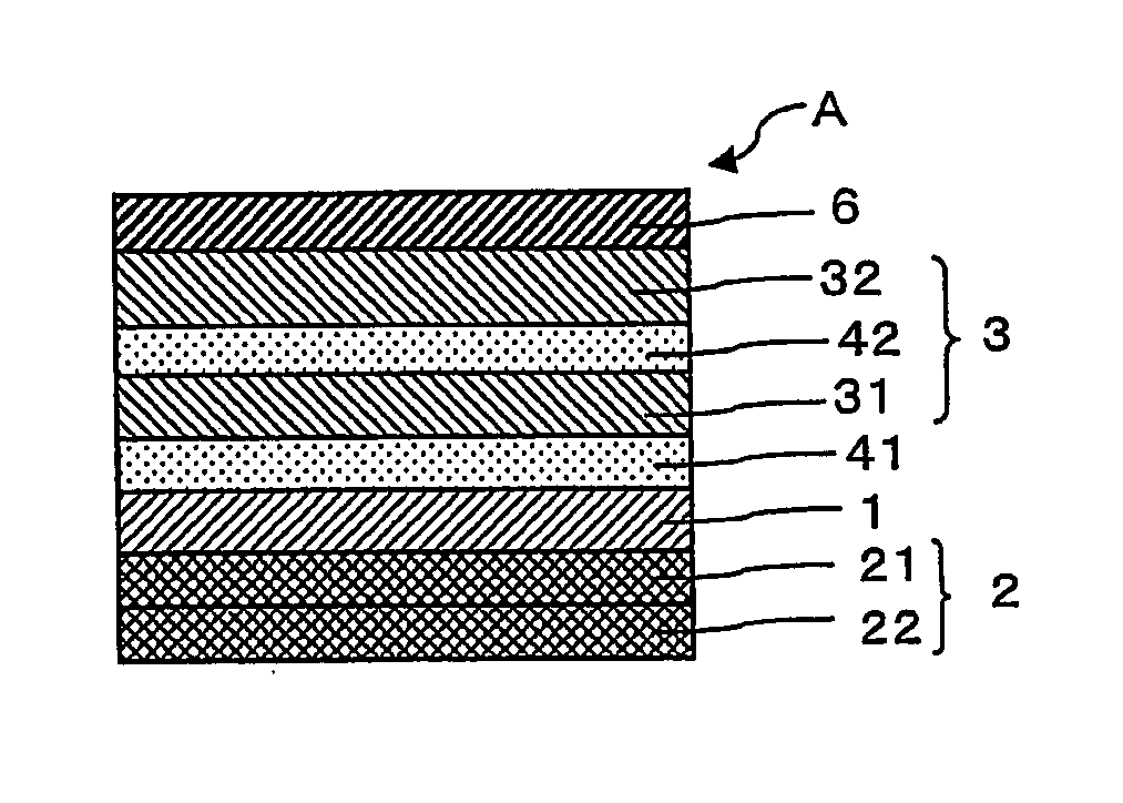
[0080]A 30 nm-thick undercoat layer (transparent dielectric thin film) of a thermosetting resin (with a light refractive index n of 1.54) composed of a melamine resin, an alkyd resin and an organosilane condensate (2:2:1 in weight ratio) was formed on one side of a film substrate made of a 25 μm-thick polyethylene terephthalate film (hereinafter referred to as “PET film”).

[0081]A 20 nm-thick first transparent conductive thin film (with a light refractive index of 2.0) of an indium-tin complex oxide was formed on the undercoat layer by a reactive sputtering method using a sintered material composed of 95% indium oxide and 6% tin oxide in a 0.4 Pa atmosphere composed of 95% by volume of argon gas and 5% by volume of oxygen gas.

[0082]A 5 nm-thick second transparent conductive thin film of an indium-tin complex oxide was formed on the first transparent conductive thin film by a reactive sputtering method using a sintered material composed of...

example 2

[0088]A transparent conductive laminated plate was prepared using the process of example 1, except that a sintered material composed of 97% by weight of indium oxide and 3% by weight of tin oxide was used instead in the process of forming the first transparent conductive thin film described in the section “Formation of Transparent Conductive Thin Films” of example 1.

example 3

[0089]A transparent conductive laminated plate was prepared using the process of example 1, except that in the process of forming the transparent conductive films described in example 1, a 200 nm-thick undercoat layer of a thermosetting resin (with a light refractive index n of 1.54) composed of a melamine resin, an alkyd resin and an organosilane condensate (2:2:1 in weight ratio) was formed instead, and then a 30 nm-thick SiO2 film (with a light refractive index of 1.46) was formed by a silica coating method including the steps of diluting a silica sol (Colcoat P, manufactured by Colcoat Co., Ltd.) with ethanol to a solid concentration of 2%, applying the diluted silica sol to the thermosetting resin layer, and then curing it after drying at 150° C. for 2 minutes.


PUM

PropertyMeasurementUnit
Massaaaaaaaaaa
Fractionaaaaaaaaaa
Fractionaaaaaaaaaa

Abstract

A transparent conductive laminate of the invention comprises: a transparent film substrate; a transparent conductive thin film provided on one side of the transparent film substrate; and a transparent base substrate bonded to another side of the transparent film substrate with a transparent pressure-sensitive adhesive layer interposed therebetween, wherein the transparent conductive thin film comprises a first transparent conductive thin film made of an indium-tin complex oxide in which SnO2/(SnO2+In2O3) is from 2 to 6% by weight and a second transparent conductive thin film made of an indium-tin complex oxide in which SnO2/(SnO2+In2O3) is more than 6% by weight and not more than 20% by weight, the first and second transparent conductive thin films are formed in this order from the transparent film substrate side, the thickness t1 of the first transparent conductive thin film and the thickness t2 of the second transparent conductive thin film have the following relationships: (1) t1 is from 10 to 30 nm; (2) t2 is from 5 to 20 nm; and (3) the sum of t1 and t2 is from 20 to 35 nm, the first transparent conductive thin film and the second transparent conductive thin film are both crystalline films, and the transparent base substrate is a transparent laminated base substrate comprising at least two transparent base films laminated to one another with a transparent pressure-sensitive adhesive layer interposed therebetween. The transparent conductive laminate has satisfactory reliability at high temperature and high humidity for touch panels and also has pen input durability and surface pressure durability.

Description

TECHNICAL FIELD[0001]The present invention relates to a transparent conductive laminate including a film substrate and a conductive thin film provided on the film substrate and having transparency in the visible light range and also relates to a touch panel therewith. The transparent conductive laminate of the invention may be used for transparent electrodes in display systems such as liquid crystal displays and electroluminescence displays and touch panels and also used for electromagnetic wave shielding or prevention of static charge of transparent products.BACKGROUND ART[0002]Touch panels can be classified according to the position detection method into an optical type, an ultrasonic type, a capacitive type, a resistive film type, and the like. In particular, the resistive film type has a relatively simple structure and thus is cost-effective so that it has come into wide use in recent years. For example, resistive film type touch panels are used for automatic teller machines (AT...

Claims


Application Information

Patent Timeline
IPC IPC(8): B32B5/00
CPCG06F3/045Y10T428/26Y10T428/265Y10T428/25Y10T428/31507Y10T428/31721Y10T428/31725Y10T428/31786Y10T428/31855G06F3/041G06F2203/04103H01B5/14
Inventor NASHIKI, TOMOTAKESUGAWARA, HIDEO
Owner NITTO DENKO CORP
Why Eureka
Try Eureka