Field effect transistor with inverted t shaped gate electrode and methods for fabrication thereof

Inactive Publication Date: 2008-10-30
GLOBALFOUNDRIES INC
View PDF99 Cites 16 Cited by
  • Summary
  • Abstract
  • Description
  • Claims
  • Application Information

AI Technical Summary

Benefits of technology

[0008]The invention includes a semiconductor structure and a plurality of methods for fabricating the semiconductor structure. The semiconductor structure in accordance with the invention comprises a semiconductor device that includes a gate electrode that has an inverted T shape. Within the context of the invention, an ‘inverted T shape’ is intended as a conventional T shape that has been rotated 180° through a horizontal axis. As a result of such rotation, a horizontal portion of an ‘inverted T shape’ is connected to a bottom of a vertical portion of the ‘inverted T shape’ rather than the top of

Problems solved by technology

One particular novel effect that may compromise operation of a semiconductor device is a short channel effect that results from inadequate control of a gate electrode over a channel region within a semiconductor device.
The gate to source and drain region capacitive effects and gate to contact stud capacitive effects are undesirable insofar as such capacitive effects contr

Method used


Image

  • Field effect transistor with inverted t shaped gate electrode and methods for fabrication thereof
  • Field effect transistor with inverted t shaped gate electrode and methods for fabrication thereof
  • Field effect transistor with inverted t shaped gate electrode and methods for fabrication thereof

Examples


Embodiment Construction

[0015]The invention, which includes a semiconductor structure and related methods for fabricating the semiconductor structure, is understood within the context of the description that follows. The description that follows is understood within the context of the drawings described above. Since the drawings are intended for illustrative purposes, the drawings are not necessarily drawn to scale.

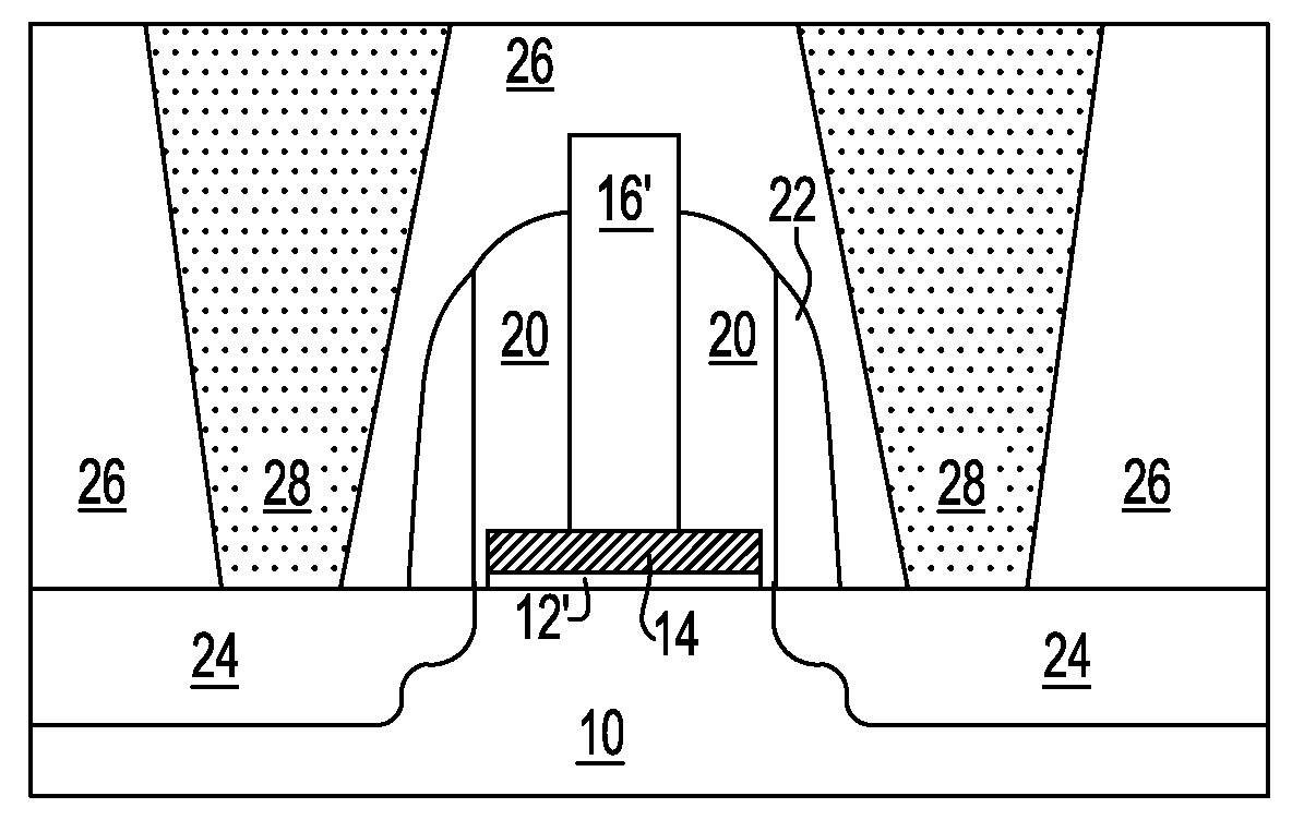
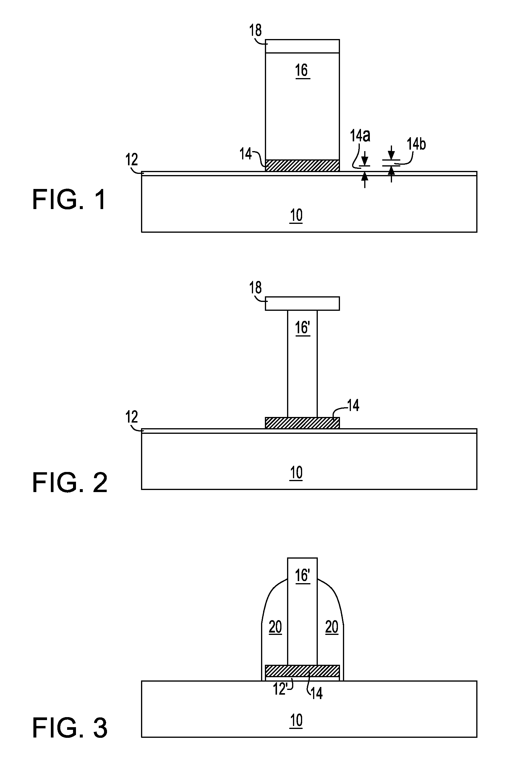
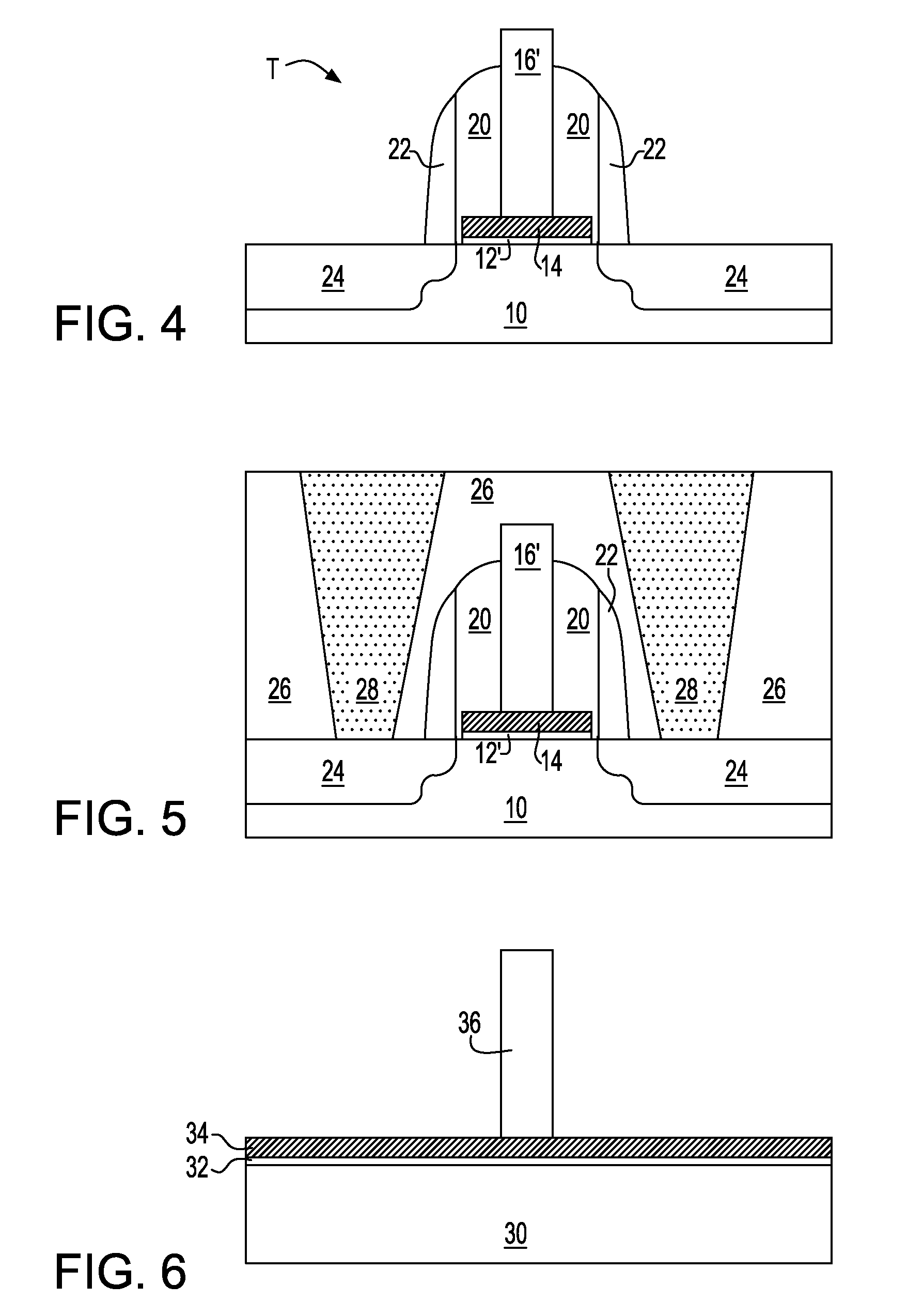
[0016]FIG. 1 to FIG. 5 show a series of schematic cross-sectional diagrams illustrating the results of progressive stages in fabricating a semiconductor structure in accordance with a particular embodiment of the invention. This particular embodiment of the invention comprises a first embodiment of the invention.

[0017]FIG. 1 shows a semiconductor substrate 10. A gate dielectric 12 is located upon the semiconductor substrate 10. A first gate electrode material layer 14 is located upon the gate dielectric 12. A second gate electrode material layer 16 is located upon the first gate electrode materi...


PUM


Abstract

A semiconductor structure includes an inverted T shaped gate electrode located over a channel region that separates a plurality of source and drain regions within a semiconductor substrate. The inverted T shaped gate electrode may comprise different gate electrode materials in a horizontal portion thereof and a vertical portion thereof. The semiconductor structure may be passivated with an inter-level dielectric (ILD) layer through which may be located and formed a plurality of vias that contact the plurality of source and drain regions. Due to the inverted T shaped gate electrode, the semiconductor structure exhibits a reduced gate electrode to via capacitance.

Description

BACKGROUND[0001]1. Field of the Invention[0002]The invention relates generally to semiconductor structures. More particularly, the invention relates to semiconductor structures with enhanced performance.[0003]2. Description of the Related Art[0004]Semiconductor structures include both active devices such as diodes and transistors, and passive devices such as resistors and capacitors. The active devices and the passive devices are connected and interconnected using patterned conductor layers that are separated by dielectric layers.[0005]As semiconductor technology has advanced, and semiconductor structure and semiconductor device dimensions have decreased, various novel effects may become more pronounced when fabricating semiconductor structures. One particular novel effect that may compromise operation of a semiconductor device is a short channel effect that results from inadequate control of a gate electrode over a channel region within a semiconductor device. Other particular nove...

Claims


Application Information

Patent Timeline
IPC IPC(8): H01L29/772
CPCH01L21/28026H01L21/28079H01L21/28114H01L29/49H01L29/495H01L29/6656H01L29/6659H01L29/7833
Inventor GREENE, BRIAN J.CLARK, WILLIAM F.DORIS, BRUCE B.
Owner GLOBALFOUNDRIES INC
Why Eureka
Try Eureka