Integrated Power Supply System Analysis System, Integrated Power Supply System Analysis Method, and Multilayer Printed Circuit Board

a power supply system and integrated technology, applied in printed circuit manufacture, instruments, computer aided design, etc., can solve the problems of affecting the performance of the lsi

Inactive Publication Date: 2008-10-30
NEC CORP
View PDF3 Cites 5 Cited by
  • Summary
  • Abstract
  • Description
  • Claims
  • Application Information

AI Technical Summary

Benefits of technology

[0009]An object of the present invention, which is proposed taking such problems as described above into consideration, is to provide an integrated power source system analysis system applicable to a multilayer printed circuit board having two or more pairs of power source—ground planes which takes interaction between LSI power source terminals with a printed circuit board provided therebetween into consideration when a plurality of LSIs are mounted on the multilayer printed circuit board, and an integrated power source system analysis method.

Problems solved by technology

Along with speed-up of electronic equipment, the problem of power source system noise of a multilayer printed circuit board mounted with an LSI becomes conspicuous.
In particular, resonance generated between power source and ground planes of a multilayer printed circuit board which is derived from power source system noise causes a power source voltage on the LSI side to fluctuate largely to degrade properties of the LSI.
The above-described conventional technique, however, has the following problems.
Another problem is that because the technique copes only with a case where one pair of power source-ground planes exists, in actual printed circuit boards, it is not applicable to an actual multilayer printed circuit board having a plurality, two or more, of pairs of power source-ground planes.

Method used


Image

  • Integrated Power Supply System Analysis System, Integrated Power Supply System Analysis Method, and Multilayer Printed Circuit Board
  • Integrated Power Supply System Analysis System, Integrated Power Supply System Analysis Method, and Multilayer Printed Circuit Board
  • Integrated Power Supply System Analysis System, Integrated Power Supply System Analysis Method, and Multilayer Printed Circuit Board

Examples


Embodiment Construction

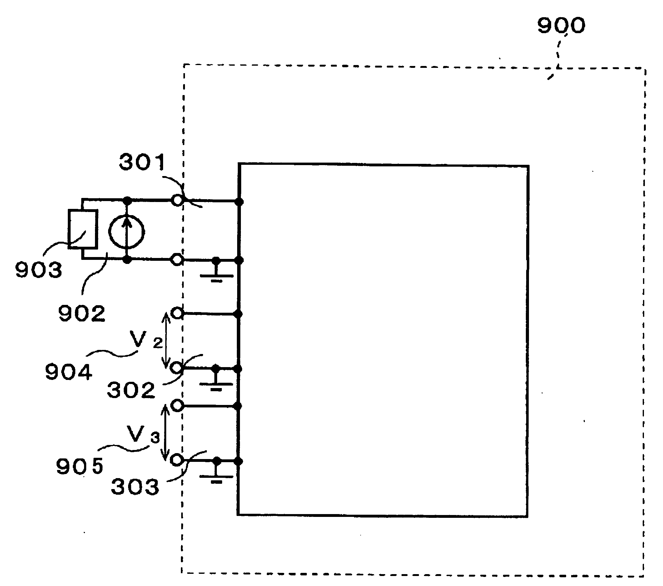
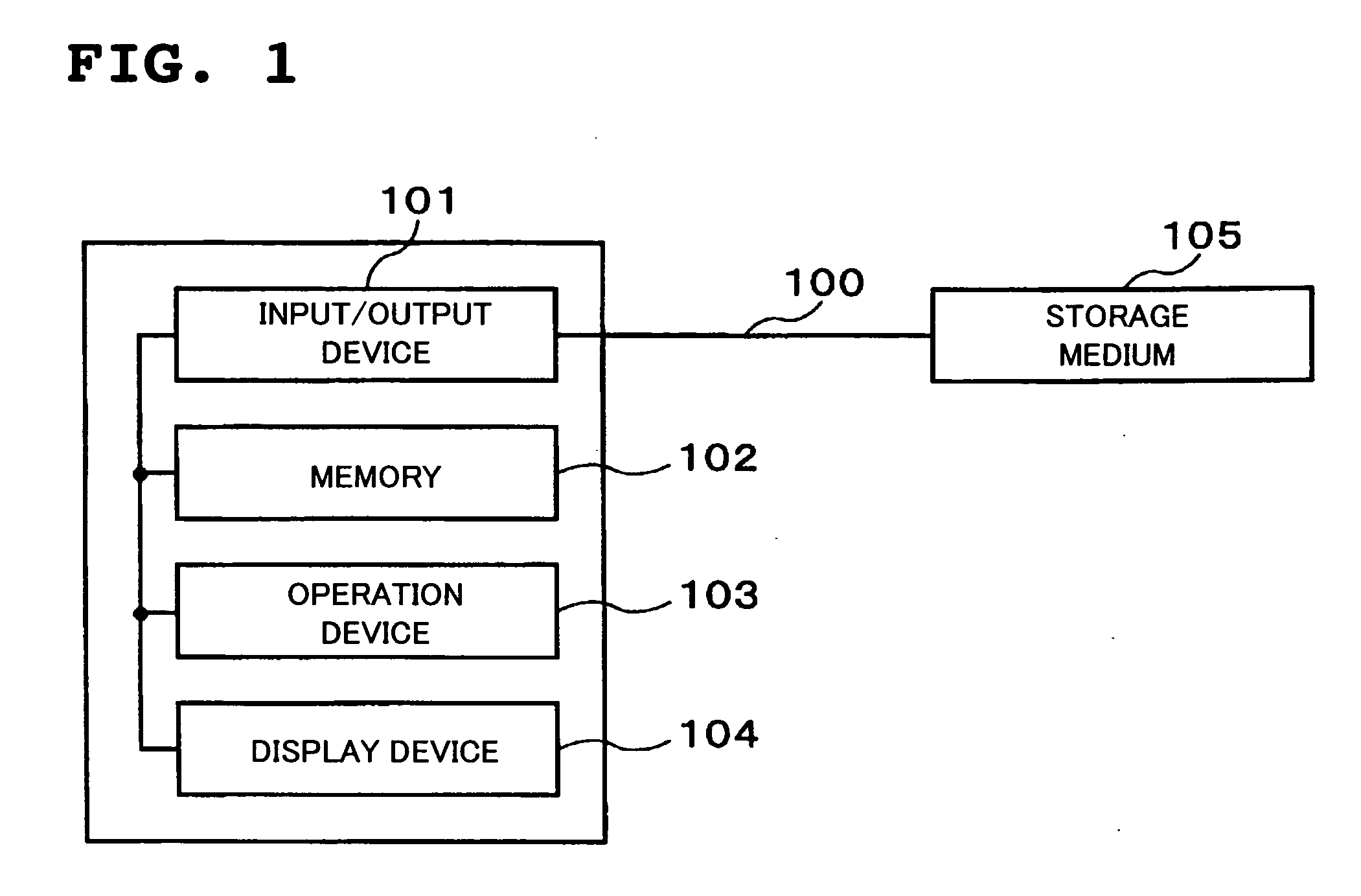
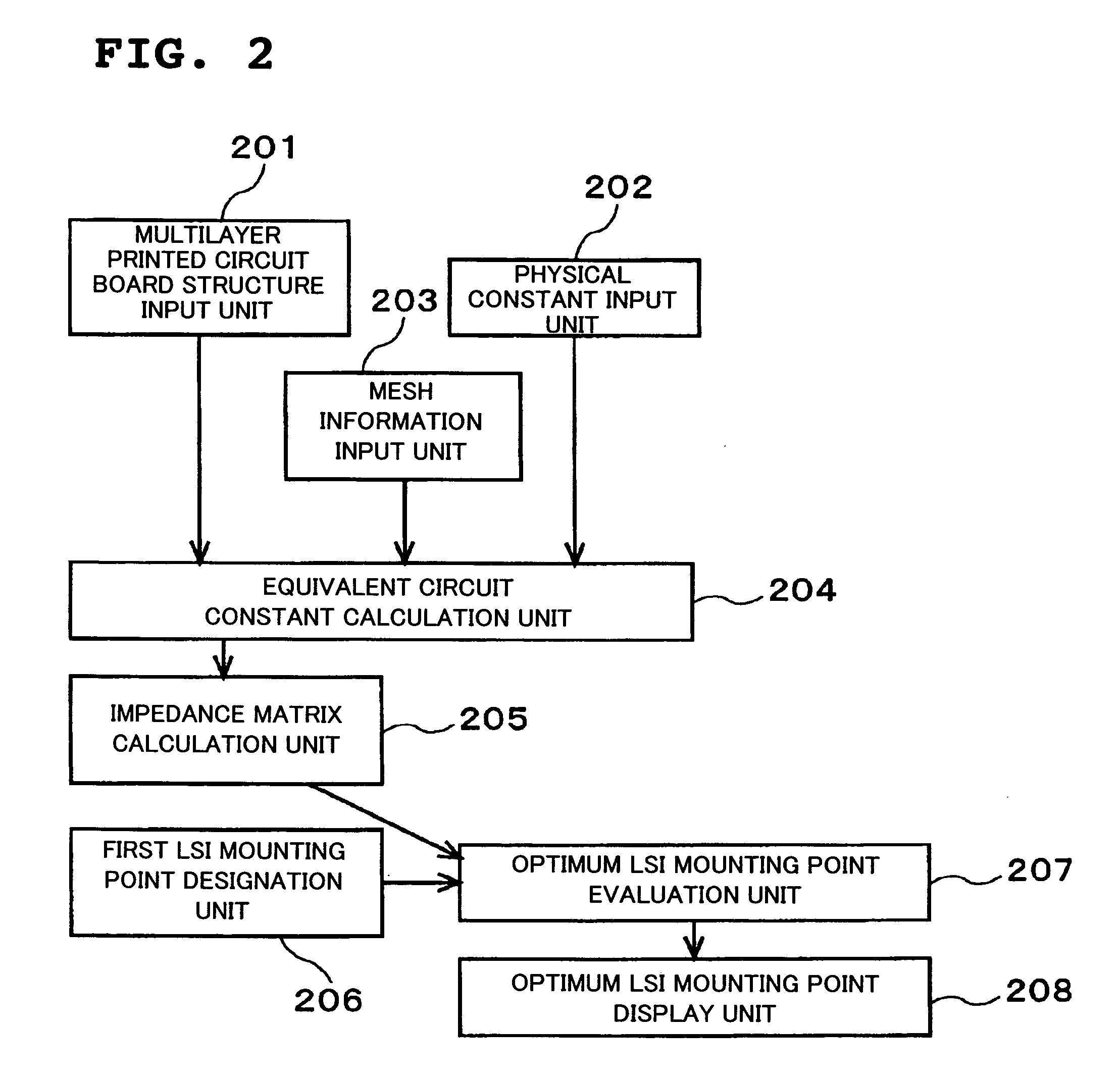
[0028]In the following, embodiments of the present invention will be specifically described with reference to the accompanying drawings. First, a first embodiment of the present invention will be described. FIG. 1 is a schematic diagram showing hardware architecture of an integrated power-source-system system according to the first embodiment of the present invention. As shown inFIG. 1, the integrated power source system analysis system according to the present embodiment includes an input / output device 101, a memory 102, an operation device 103 and a display device 104, with the input / output device 101 connected to a storage device 105 through a bus 100. In addition, FIG. 2 is a block diagram functionally showing the structure of the integrated power source system analysis system according to the present embodiment. The integrated power source system analysis system according to the present embodiment includes a multilayer printed circuit board structure information input unit 201,...


PUM


Abstract

Information related to a structure of a multilayer printed circuit board, a physical constant and a mesh is input (Step S701) to generate an equivalent circuit model of the multilayer printed circuit board (Step S702). A transfer matrix is generated with an LSI power source terminal mounting candidate point of the uppermost layer as an input and an LSI power source terminal mounting candidate point of the lowermost layer as an output (Step S703) and the transfer matrix is converted into an impedance matrix (Step S704). Here, a first LSI mounting point is input (Step S705) to select an optimum LSI mounting point (Step S706) and the optimum LSI mounting point and the remaining LSI mounting candidate points are sequentially output (Step S707).

Description

FIELD OF THE INVENTION[0001]The present invention relates to an integrated power source system analysis system integrating power design of an LSI and a multilayer printed circuit board which enables interconnection of power source systems of a plurality of LSIs (Large Scale Integrated Circuit), an integrated power source system analysis method and a multilayer printed circuit board.DESCRIPTION OF THE RELATED ART[0002]Along with speed-up of electronic equipment, the problem of power source system noise of a multilayer printed circuit board mounted with an LSI becomes conspicuous. In particular, resonance generated between power source and ground planes of a multilayer printed circuit board which is derived from power source system noise causes a power source voltage on the LSI side to fluctuate largely to degrade properties of the LSI. Accordingly, in designing an LSI, it is essential to make design taking information of a multilayer printed circuit board into consideration.[0003]As ...

Claims


Application Information

Patent Timeline
Patent Type & Authority Applications(United States)
IPC IPC(8): G06F17/50H05K1/11H05K3/00H05K3/30H05K3/46
CPCG06F17/5036H05K1/112H05K3/0005H05K3/303G06F30/367
Inventor KOBAYASHI, NAOKIHARADA, TAKASHI
Owner NEC CORP
Why Eureka
Try Eureka