JFET Having a Step Channel Doping Profile and Method of Fabrication

a junction field effect transistor and doping profile technology, applied in the direction of transistors, electrical devices, semiconductor devices, etc., can solve the problems of inability to achieve optimal performance of transistors during on-state, and achieve the effect of substantially reducing the disadvantages and eliminating the problems of prior junction field effect transistors

Inactive Publication Date: 2008-11-06
DSM SOLUTIONS
View PDF8 Cites 124 Cited by
  • Summary
  • Abstract
  • Description
  • Claims
  • Application Information

AI Technical Summary

Benefits of technology

[0003]In accordance with the present invention, the disadvantages and problems associated with prior junction field effect transistors have been substantially reduced or eliminated.

Problems solved by technology

As a result, the performance of the transistor is not optimal during an ON-state and / or OFF-state of operation.

Method used


Image

  • JFET Having a Step Channel Doping Profile and Method of Fabrication
  • JFET Having a Step Channel Doping Profile and Method of Fabrication
  • JFET Having a Step Channel Doping Profile and Method of Fabrication

Examples


Embodiment Construction

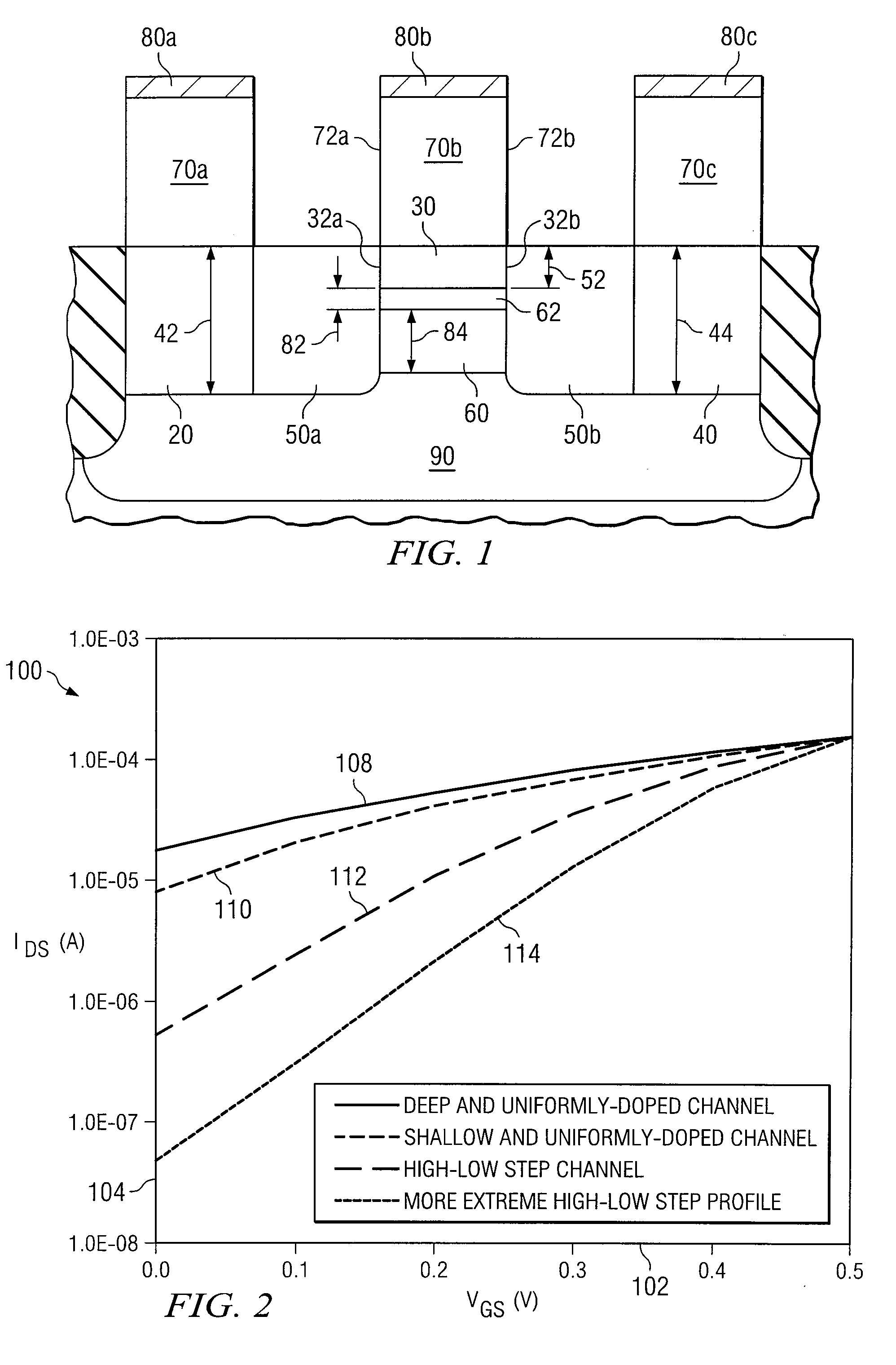
[0013]FIG. 1 illustrates a semiconductor device 10 according to a particular embodiment of the present invention. As shown in FIG. 1, semiconductor device 10 includes a source region 20, a gate region 30, a drain region 40, link regions 50a-b, a first channel region 60, a second channel region 62, polysilicon regions 70a-c, contacts 80a-c, and a substrate 90. These regions are not necessarily drawn to scale. Semiconductor device 10 comprises a junction field effect transistor (JFET). When appropriate voltages are applied to contacts 80 of semiconductor device 10, a current flows through channel regions 60 and 62 between source region 20 and drain region 40. By providing distinct channel regions 60 and 62, as described in greater detail below, semiconductor device 10 exhibits enhanced performance characteristics in an OFF-state and / or an ON-state of operation.

[0014]Substrate 90 represents bulk semiconductor material to which dopants can be added to form various conductivity regions (...


PUM


Abstract

A junction field effect transistor comprises a semiconductor substrate, a source region formed in the substrate, a drain region formed in the substrate and spaced apart from the source region, and a gate region formed in the substrate. The transistor further comprises a first channel region formed in the substrate and spaced apart from the gate region, and a second channel region formed in the substrate and between the first channel region and the gate region. The second channel region has a higher concentration of doped impurities than the first channel region.

Description

TECHNICAL FIELD OF THE INVENTION[0001]This invention relates in general to semiconductor devices, and more particularly to a junction field effect transistor having a step channel doping profile.BACKGROUND OF THE INVENTION[0002]Prior junction field effect transistors use a single channel region to conduct current between the source and drain regions. This single channel region comprises a relatively uniform concentration of doped impurities. As a result, the performance of the transistor is not optimal during an ON-state and / or OFF-state of operation.SUMMARY OF THE INVENTION[0003]In accordance with the present invention, the disadvantages and problems associated with prior junction field effect transistors have been substantially reduced or eliminated.[0004]In accordance with one embodiment of the present invention, a junction field effect transistor comprises a semiconductor substrate. A source region, drain region, and gate region are formed in the substrate. The transistor furthe...

Claims


Application Information

Patent Timeline
Patent Type & Authority Applications(United States)
IPC IPC(8): H01L21/337H01L29/80
CPCH01L29/1058H01L29/66901H01L29/808
Inventor SONKUSALE, SACHIN R.ZHANG, WEIMINKAPOOR, ASHOK K.
Owner DSM SOLUTIONS
Why Eureka
Try Eureka