Semiconductor device and method for manufacturing semiconductor device
Active Publication Date: 2008-11-06
SHARP KK
View PDF6 Cites 12 Cited by
Summary
Abstract
Description
Claims
Application Information
AI Technical Summary
This helps you quickly interpret patents by identifying the three key elements:
Problems solved by technology
Method used
Benefits of technology
Benefits of technology
[0016]It is an object of the present invention to provide a semiconductor device and a method for manufacturing a semiconductor device, both of which make it possible to suppress electromagnetic interference between a secondary wire and an electronic circuit and suppress the curvature of a wafer even in cases where the secondary wire and the electronic circuit overlap each other, and to reduce the risk of occurrence of chipping in a dicing step.
Problems solved by technology
This may cause problems with delays in electrical signals inputted and outputted via electrode pads.
Moreover, this may cause a problem of inability to ensure a wire width appropriate for an electrical current required by the electronic circuit or a problem of deterioration in yield in the step of forming secondary wires.
Furthermore, according to the technique disclosed in Patent Document 1, as the distance between secondary wires shortens, the parasitic capacitance of an insulating layer existing between the secondary wires increases.
This may cause wiring delays.
However, the semiconductor device disclosed in Patent Document 3 suffers from a problem of high risk of occurrence of chipping in a dicing step.
However, in cases where an insulating layer, or an organic insulating layer in particular, is formed thickly in an area near the scribe line, the formation of the insulating layer alone can be a factor that causes chipping in the dicing step.
This is because the chipping is attributed to clogging of a dicing blade.
The formation of the insulating layer in an area near the scribe line causes the semiconductor device to have more incidence of clogging of the dicing blade.
Further, the semiconductor device disclosed in Patent Document 3 suffers from a problem with an increase in the curvature of a wafer.
Therefore, the technique disclosed in Patent Document 3 merely arranged such that the sealing resin layer is provided with the holes has difficulty in bringing about a sufficiently great effect of suppressing the curvature of a wafer.
However, the formation of a large number of such holes undesirably complicates the structure of the semiconductor device.
Method used
Image
Click on the blue label to locate the original text in one second.
Reading with bidirectional positioning of images and text.
Examples
embodiment 1
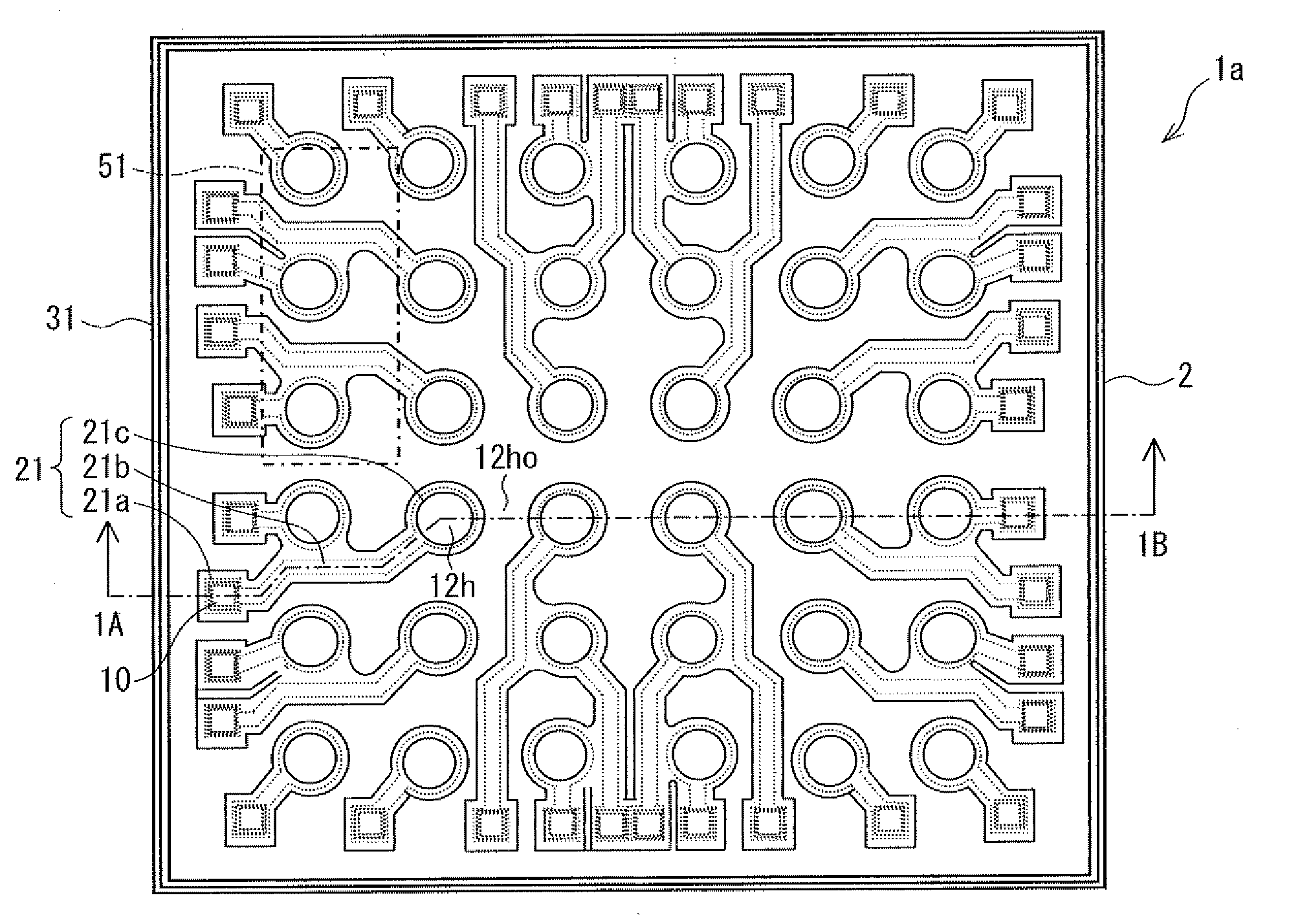
[0109]A semiconductor device according to an embodiment of the present invention will be described below with reference to FIGS. 1(a) and 1(b).
[0110]FIG. 1(a), showing an embodiment of the present invention, is a plan view showing an arrangement of a semiconductor device 1a. Further, FIG. 1(b) is a cross-sectional view taken along the line 1A-1B of FIG. 1(a).
[0111]The semiconductor device 1a of FIG. 1(a) includes a semiconductor chip 2 having a circuit-forming surface, having an electronic circuit section (electronic circuit) 51 formed thereon, on which a plurality of peripherally-disposed electrode pads 10 are provided. It should be noted that the semiconductor chip 2 and the semiconductor chips 3 to 9 described below are members having the same functions. The electrode pads 10 make an electrical connection between the electronic circuit section 51 formed on the semiconductor chip 2 and an externally-connected circuit, and are connected via primary wires (not shown) provided inside...
embodiment 2
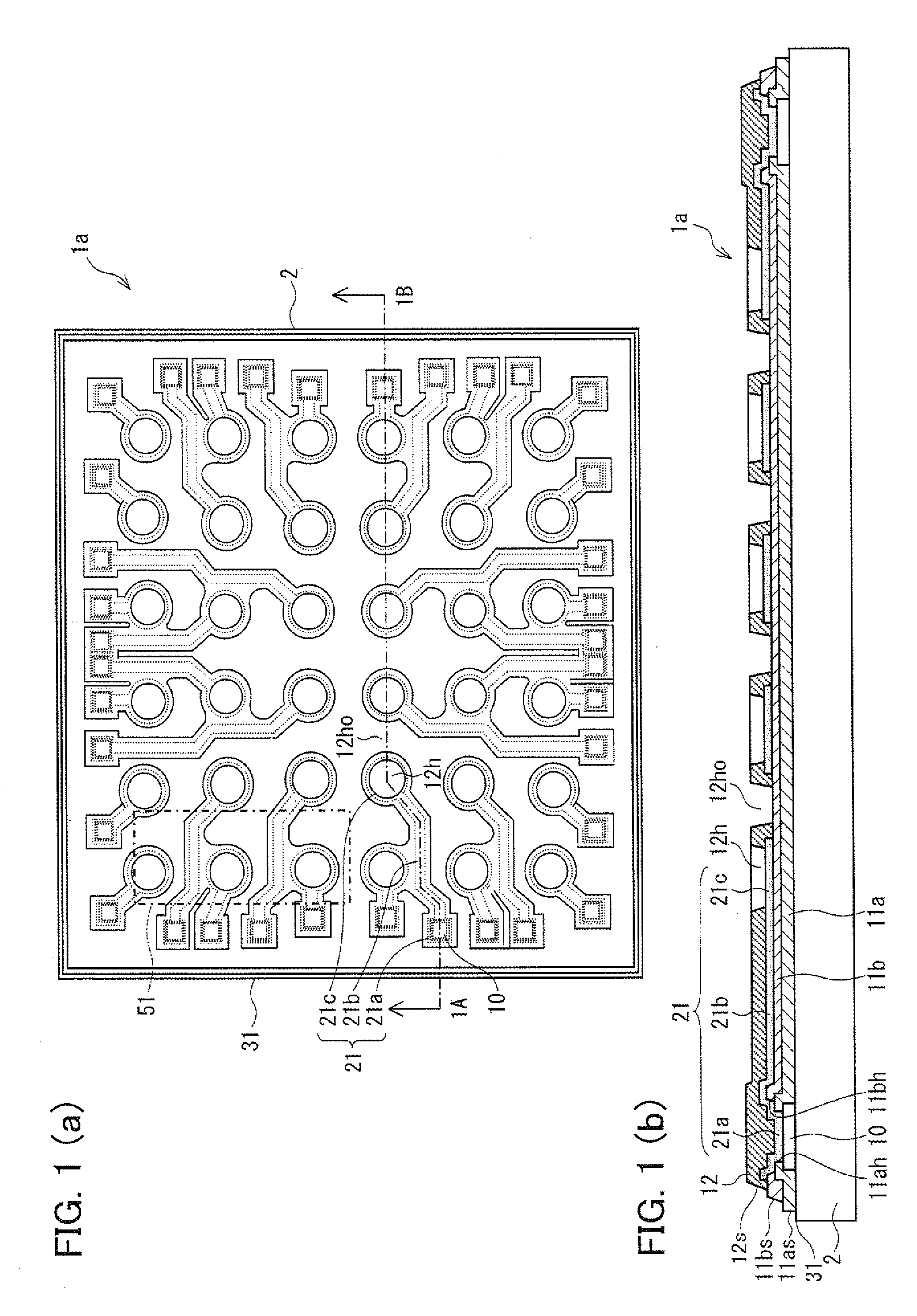
[0150]A semiconductor device according to another embodiment of the present invention will be described below with reference to FIGS. 2(a) and 2(b).
[0151]FIG. 2(a), showing an embodiment of the present invention, is a plan view showing an arrangement of a semiconductor device 1b. Further, FIG. 2(b) is a cross-sectional view taken along the line 2A-2B of FIG. 2(a).
[0152]The semiconductor chip 2 of the semiconductor device 1a of FIGS. 1(a) and 1(b) is arranged such that the depression 12ho of the upper insulating layer 12 is provided in the first secondary-wire-free area excluding the first secondary-wire-containing area and the area therearound.
[0153]Meanwhile, the semiconductor chip 3 of the semiconductor device 1b of FIGS. 2(a) and 2(b) is provided with a side wall 11bs′ of the lower insulating layer 11b instead of the depression 12ho.
[0154]The lower insulating layer 11b is made of PBO so as to have a thickness of 10 μm. Further, the opening 11bh is provided above the opening 11ah...
embodiment 3
[0173]A semiconductor device according to another embodiment of the present invention will be described below with reference to FIGS. 3(a) and 3(b).
[0174]FIG. 3(a), showing an embodiment of the present invention, is a plan view showing an arrangement of a semiconductor device 1c. Further, FIG. 3(b) is a cross-sectional view taken along the line 3A-3B of FIG. 3(a).
[0175]The semiconductor device 1c of FIGS. 3(a) and 3(b) includes a semiconductor chip 4 provided with lower insulating layers 11a and 11b and secondary wires 21 that are made of the same materials as, and formed as thickly as, those of the semiconductor device 1b of FIGS. 2(a) and 2(b), and is arranged such that the lower insulating layer 11b is provided with a side wall 11bs′. Further, the semiconductor device 1c of FIGS. 3(a) and 3(b) is arranged such that the semiconductor chip 4 is provided with an upper insulating layer 12 that is made of the same material as, and formed as thickly as, in the semiconductor device 1a o...
PUM
Abstract
A semiconductor device according to the present invention has a semiconductorchip provided with an insulating layer formed so as to be thinner in a first secondary-wire-free area than in a first secondary-wire-containing area. Further, the semiconductorchip has an edge extending further outward than a side wall, which severs as an edge of an upper insulating layer, in an extending direction of a circuit-forming surface of the semiconductor chip on which electrode pads are provided. This makes it possible to provide a semiconductor device capable of suppressing electromagnetic interference between a secondary wire and an electronic circuit of a semiconductor chip and the curvature of a wafer even in the case of overlap between the secondary wire and the electronic circuit, and of reducing the risk of occurrence of chipping in a dicing step.
Description
[0001]This Nonprovisional application claims priority under 35 U.S.C. § 119(a) on Patent Application No. 120202 / 2007 filed in Japan on Apr. 27, 2007, Patent Application No. 029697 / 2008 filed in Japan on Feb. 8, 2008, Patent Application No. 111047 / 2008 filed in Japan on Apr. 22, 2008, the entire contents of which are hereby incorporated by reference.FIELD OF THE INVENTION[0002]The present invention relates to (i) a semiconductor device including a semiconductor chip having electrode pads, external connection terminals, and secondary wires (i.e., rewiring layers) and (ii) a method for manufacturing a semiconductor device.BACKGROUND OF THE INVENTION[0003]In recent years, there has existed a semiconductor device which, in order to be connected to a circuit formed outside thereof, includes a semiconductor chip having the following structure.[0004]That is, the semiconductor chip has a circuit-forming surface provided with electrode pads, secondary wires, and external connection terminals ...
Claims
Application Information
Patent Timeline
Application Date:The date an application was filed.
Publication Date:The date a patent or application was officially published.
First Publication Date:The earliest publication date of a patent with the same application number.
Issue Date:Publication date of the patent grant document.
PCT Entry Date:The Entry date of PCT National Phase.
Estimated Expiry Date:The statutory expiry date of a patent right according to the Patent Law, and it is the longest term of protection that the patent right can achieve without the termination of the patent right due to other reasons(Term extension factor has been taken into account ).
Invalid Date:Actual expiry date is based on effective date or publication date of legal transaction data of invalid patent.

