Image capturing system, signal processing circuit, and signal processing method

a technology of image capturing and signal processing, applied in the direction of color signal processing circuits, television systems, color television details, etc., can solve problems such as the inability to appropriately correct signals

Inactive Publication Date: 2008-11-06
CANON KK
View PDF13 Cites 34 Cited by
  • Summary
  • Abstract
  • Description
  • Claims
  • Application Information

AI Technical Summary

Benefits of technology

[0016]The present invention also provides for accurately canceling fixed pattern noise generated by an unbalanced electrical characteristic of a read circuit or a circuit included in a pixel in an image sensing apparatus including a plurality of pixels having different pixel structures.
[0025]According to the present invention, it is possible to satisfactorily correct a signal even when the dark current varies between pixels.
[0026]According to the present invention, it is also possible to accurately cancel fixed pattern noise generated by an unbalanced electrical characteristic of a read circuit or a circuit included in a pixel in an image sensing apparatus including a plurality of pixels having different pixel structures.

Problems solved by technology

It is impossible to appropriately correct a signal when the influence of the dark current is large.

Method used


Image

  • Image capturing system, signal processing circuit, and signal processing method
  • Image capturing system, signal processing circuit, and signal processing method
  • Image capturing system, signal processing circuit, and signal processing method

Examples


working example 1

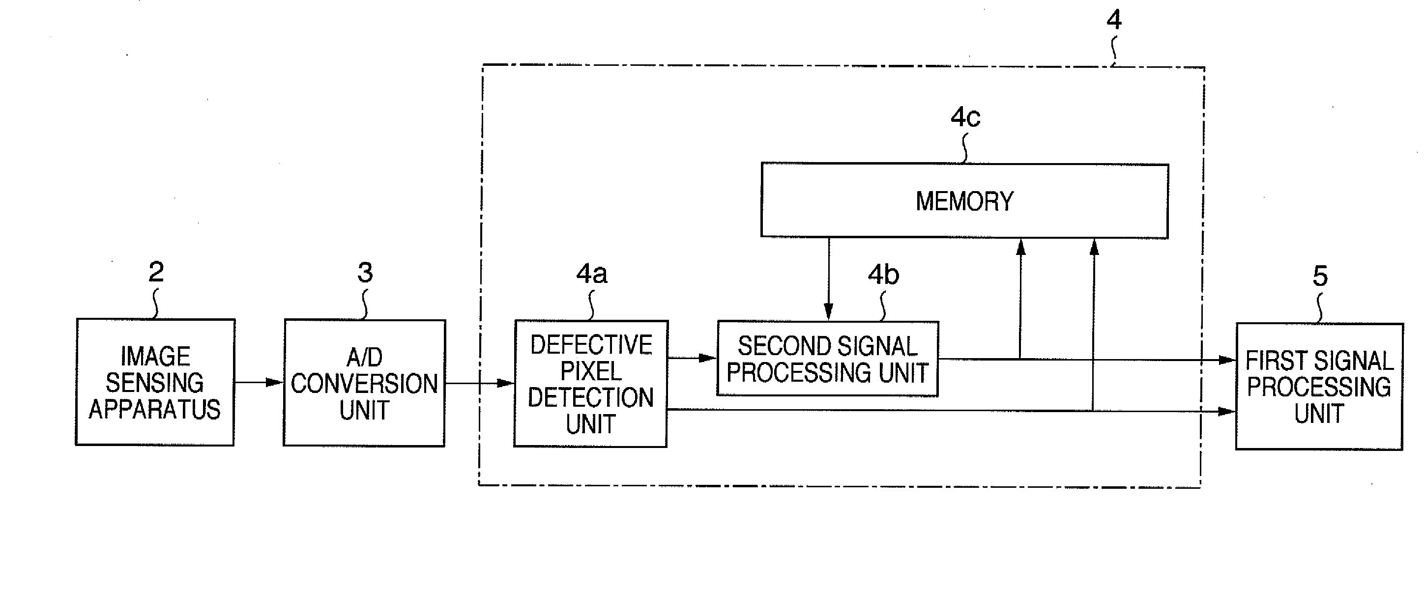
[0060]In this example, four transfer gates share an amplifying element. The potential of the gate of an amplification transistor functioning as a common amplifying element is changed on the basis of charges from the four transfer gates.

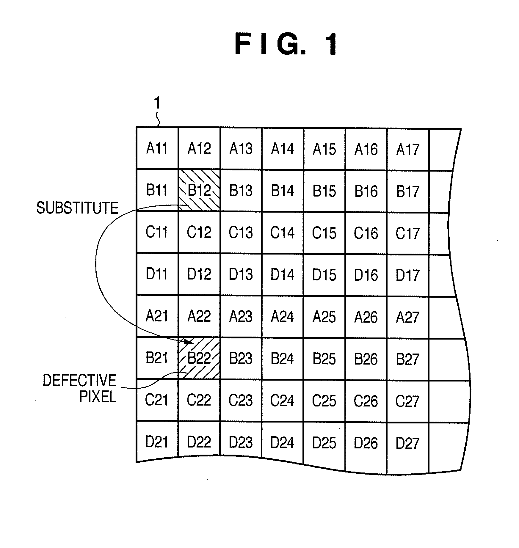
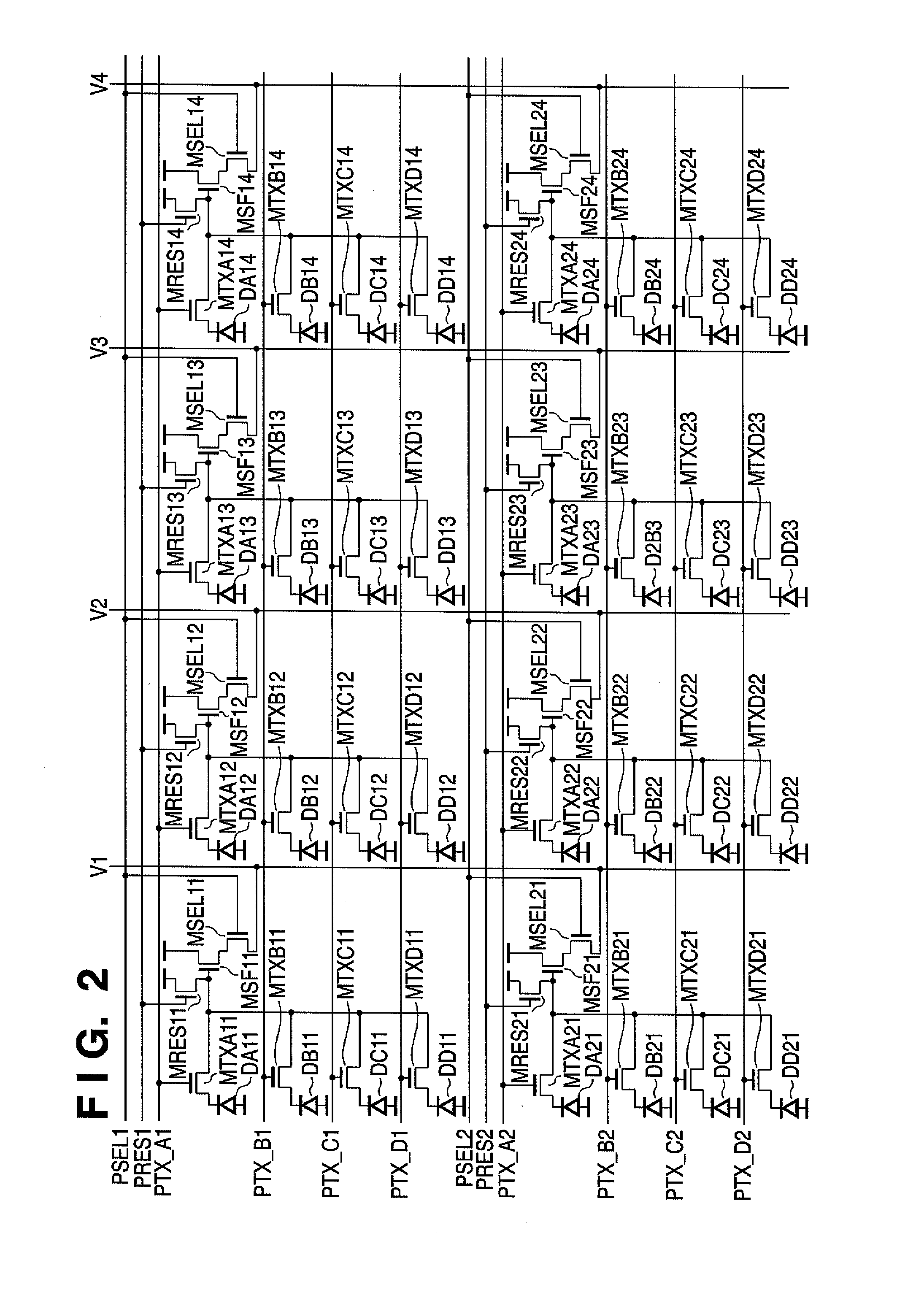
[0061]In this example, a plurality of transfer transistors (including transfer gates) share a reset transistor and a pixel selection transistor. FIG. 2 is an equivalent circuit. FIG. 3 is a view showing the pixel layout. FIG. 4 is a sectional view taken along a line X-X′ in FIG. 3. These drawings illustrate only specific pixels. However, a number of pixels may be arranged in the row and column directions.

[0062]The circuit arrangement of the upper left pixel block (A11 to D11 shown in FIG. 1) will be described with reference to FIG. 2. The remaining pixel blocks have the same circuit arrangement as that of the upper left pixel block.

[0063]Photodiodes DA11 to DD11 have the same arrangement as that of a photoelectric conversion element in an effective ar...

working example 2

[0088]In this example, a signal correction method related to an optical black pixel for outputting a black reference signal (dark reference signal) will be described. FIG. 8 shows the pixel layout of an image sensing apparatus.

[0089]Referring to FIG. 8, reference numeral 1 denotes a pixel; 10, a first OB region (vertical OB region); 11, a second OB region (horizontal OB region); and 12, an effective area adjacent to the optical black regions 10 and 11. A dark current is corrected by generating a black reference signal using these OB regions. When a dark signal distribution (vertical shading) generated by the influence of a dark current exists in the vertical direction, the shading can be reduced by executing correction using signals from the horizontal OB region 11. When a dark signal distribution (horizontal shading) generated by the influence of a dark current exists in the horizontal direction, correction can be done using signals from the vertical OB region 10.

[0090]FIG. 9 is a ...

working example 3

[0093]This example is related to a signal correction method when a pixel defect is generated in a vertical OB region 10. This example can also use the block diagram of the image sensing apparatus in FIG. 9.

[0094]FIG. 11 is an enlarged view of the vertical OB region 10. The same arrangement as in Working Example 1 is usable as a pixel layout, as in Working Example 2.

[0095]In Working Example 3, a pixel row is further divided into a plurality of regions (block 1, block 2, . . . ) in the horizontal direction. The signals from a plurality of pixels in each region are averaged and recorded in a memory. Simultaneously, pieces of address information representing the pixel row and the divided regions are recorded.

[0096]An averaging processing unit 4d in FIG. 9 adds the signals from a plurality of pixels in each region divided in the horizontal direction, calculates the average value, and records it in a memory 4c together with address information. The memory 4c records the average signal of ...


PUM


Abstract

An image capturing system includes a signal correction unit which corrects a signal output from a defective pixel in an optical black region based on a signal output from a normal pixel. The optical black region has a plurality of pixel blocks. Each of the plurality of pixel blocks has a plurality of pixels each including one or more elements which have the same functions as in the remaining pixels and which have relative positions different from the remaining pixels. The signal correction unit corrects the signal output from the defective pixel in the optical black region based on a signal output from a normal pixel which is included in another pixel block different from the pixel block of the defective pixel in the optical black region and includes one or more elements having the same functions and same relative positions as in the defective pixel.

Description

BACKGROUND OF THE INVENTION[0001]1. Field of the Invention[0002]The present invention relates to an image capturing system, signal processing circuit, and signal processing method.[0003]2. Description of the Related Art[0004]Many image capturing systems such as a digital camera, video camera, copying machine, or a facsimile apparatus incorporate an image sensing apparatus in which pixels each including a photoelectric conversion element are arrayed one- or two-dimensionally. The image sensing apparatuses include a CCD image sensing apparatus or an amplifying image sensing apparatus having amplifying elements in the pixel region.[0005]Recent image sensing apparatuses tend to increase the number of pixels. As the area of one pixel decreases, the area of a photoelectric conversion element also tends to decrease. That a photoelectric conversion element has a smaller area indicates that an amount of incident light per pixel becomes small. In, for example, an amplifying image sensing appa...

Claims


Application Information

Patent Timeline
Patent Type & Authority Applications(United States)
IPC IPC(8): H04N9/64H04N5/361H04N5/367
CPCH04N5/361H04N5/367H04N25/63H04N25/68
Inventor TAKENAKA, SHINTAROSONODA, KAZUHIROKITANI, KAZUNARI
Owner CANON KK
Why Eureka
Try Eureka