Semiconductor wafer with assisting dicing structure and dicing method thereof

a technology of dicing structure and dicing method, which is applied in the direction of semiconductor devices, semiconductor/solid-state device details, electrical apparatus, etc., can solve the problems of aggravated cracking, fatal defects, and stress in the dicing lane regions

Active Publication Date: 2008-11-13
TAIWAN SEMICON MFG CO LTD
View PDF12 Cites 43 Cited by
  • Summary
  • Abstract
  • Description
  • Claims
  • Application Information

AI Technical Summary

Problems solved by technology

However, stress may be created in the dicing lane regions during the sawing process.
The created stress is a source of crack propagating into integrated circ...

Method used


Image

  • Semiconductor wafer with assisting dicing structure and dicing method thereof
  • Semiconductor wafer with assisting dicing structure and dicing method thereof
  • Semiconductor wafer with assisting dicing structure and dicing method thereof

Examples


Embodiment Construction

[0021]The following description is of the best-contemplated mode of carrying out the invention. This description is provided for the purpose of illustrating the general principles of the invention and should not be taken in a limiting sense. The scope of the invention is best determined by reference to the appended claims. Embodiments of a semiconductor wafer with an assistant dicing structure and a dicing method thereof are described with reference to the accompanying drawings.

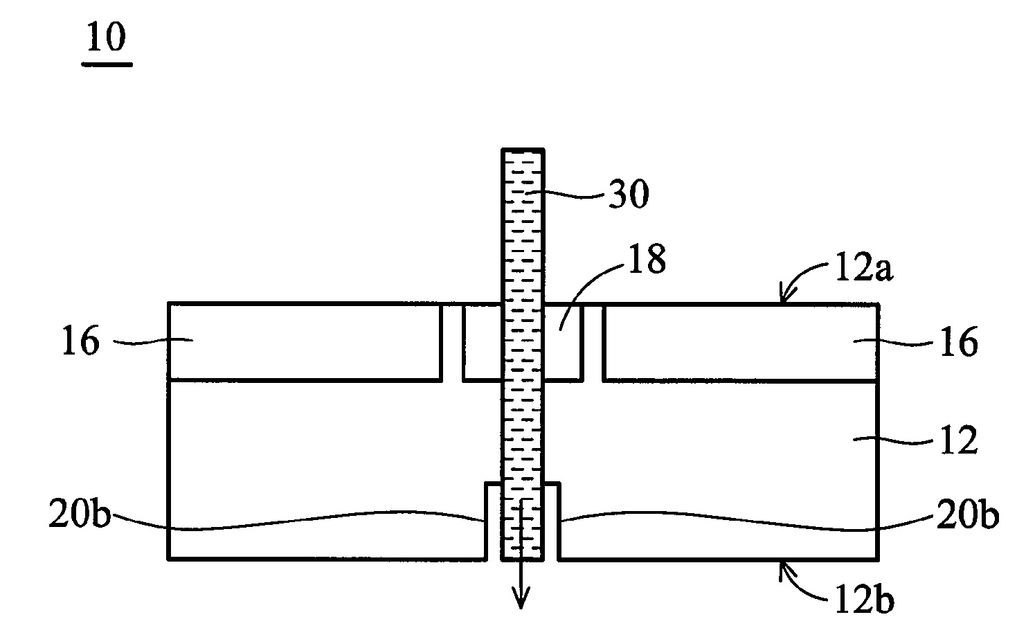
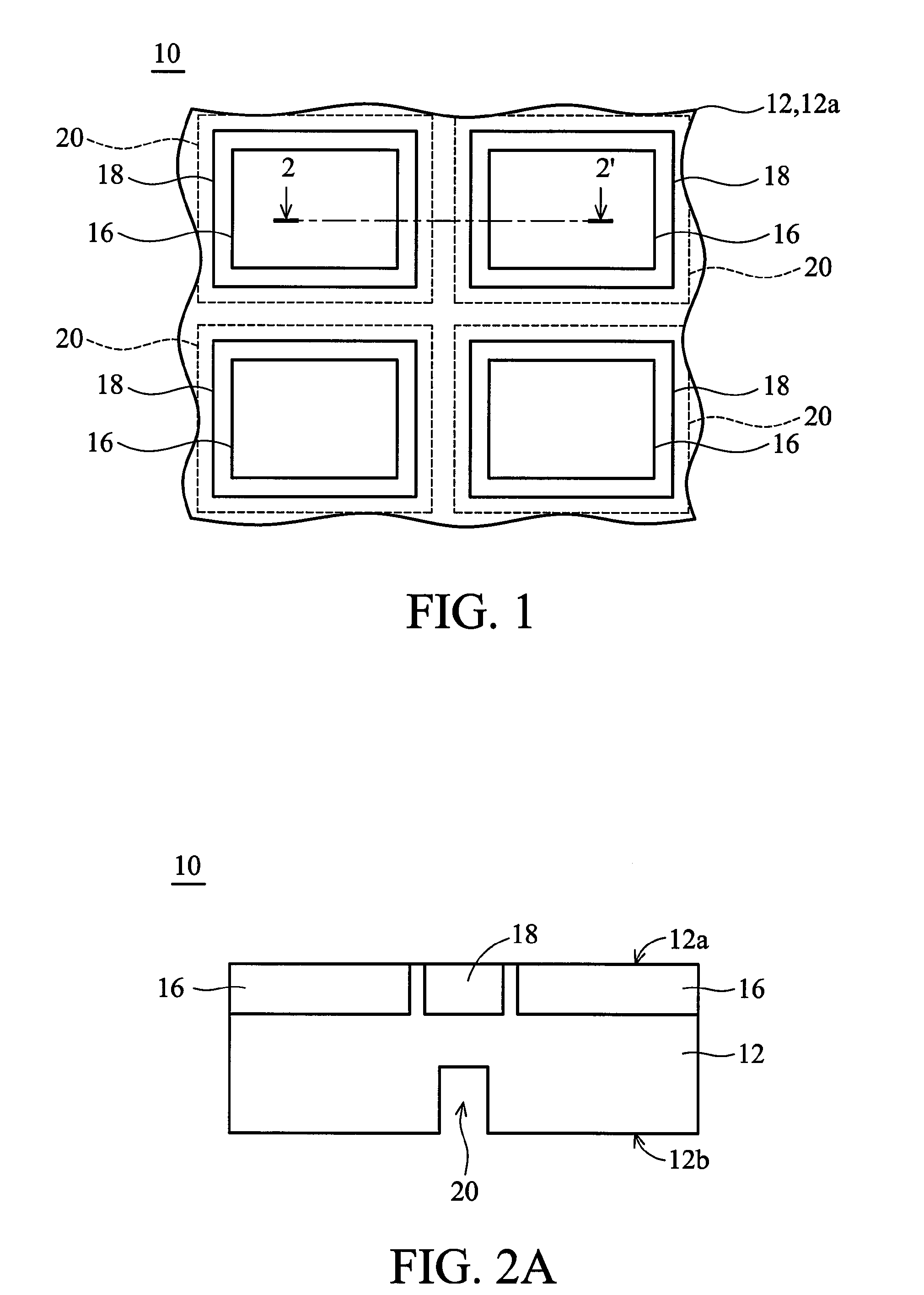
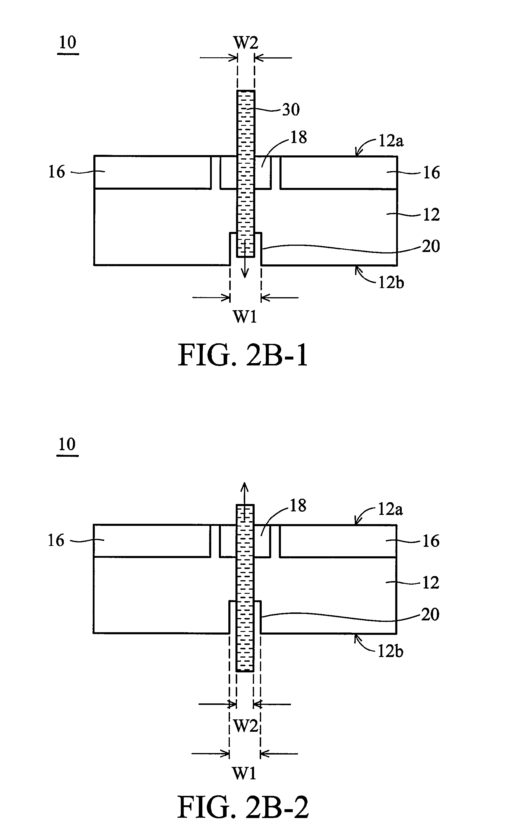
[0022]FIGS. 1 and 2A illustrate an embodiment of a semiconductor wafer with an assisting dicing structure, in which FIG. 1 is a plan view and FIG. 2A is a cross section along line 2-2′ shown in FIG. 1. The semiconductor wafer 10 comprises a substrate 12. The substrate 12 may comprise silicon, germanium, silicon germanium, GaAs, InAs, InP and other Group III-V semiconductor compounds. The substrate 12 may also comprise layered semiconductor such as Si / SiGe. Compound semiconductors such as GaAs and InP possess ...


PUM


Abstract

A semiconductor wafer with an assisting dicing structure. The wafer comprises a substrate having a front surface and a rear surface. The front surface of the substrate comprises at least two device regions separated by at least one dicing lane. The rear surface of the substrate comprises at least one pre-dicing trench formed therein and substantially aligned with the dicing lane. A method for dicing a semiconductor wafer is also disclosed.

Description

BACKGROUND OF THE INVENTION[0001]1. Field of the Invention[0002]The invention relates to semiconductor technology and in particular to a semiconductor wafer with an assisting dicing structure and a dicing method thereof capable of preventing cracks from forming or propagating in the integrated circuits of the wafer during dicing.[0003]2. Description of the Related Art[0004]In the manufacture of microelectronic devices, a plurality of integrated circuits are formed on a semiconductor wafer, usually comprised primarily of silicon, by conventional semiconductor fabrication techniques, such as photolithography, film deposition and etching, and material doping. Thus, a semiconductor wafer can comprise a plurality of integrated circuits formed on a surface area of the wafer and arranged in rows and columns with the periphery of each integrated circuit being rectangular.[0005]Typically, individual integrated circuits are formed by sawing or dicing through the wafer into rectangular discret...

Claims


Application Information

Patent Timeline
IPC IPC(8): H01L23/544H01L21/00
CPCB28D5/022H01L21/78H01L23/562H01L2924/0002H01L2924/00
Inventor CHEN, HSIEN-WEIHSU, SHIH-HSUN
Owner TAIWAN SEMICON MFG CO LTD
Why Eureka
Try Eureka