Method of fabricating electron emission source, electron emission device, and electron emission display device including the electron emission device

a technology of electron emission source and electron emission display device, which is applied in the field of electron emission, can solve the problems of complex manufacturing process, difficult to achieve improved electron emission efficiency, and widespread use of fed-type electron emission device, and achieve the effect of improving electron emission efficiency and simplifying manufacturing processes

Inactive Publication Date: 2008-11-13
SAMSUNG SDI CO LTD
View PDF5 Cites 6 Cited by
  • Summary
  • Abstract
  • Description
  • Claims
  • Application Information

AI Technical Summary

Benefits of technology

[0011]Aspects of the present invention provide a method of fabricating an electron emission source which can attain improved electron emission efficiency and has simplified manufacturing processes.

Problems solved by technology

When an electron emission source formed of a carbon-based material is fabricated using a printing method with a known paste or direct epitaxy by way of chemical vapor deposition (CVD), it is difficult to attain improved electron emission efficiency, or the manufacturing process is complicated.
These are obstacles in realizing widespread use of the FED type electron emission devices.

Method used


Image

  • Method of fabricating electron emission source, electron emission device, and electron emission display device including the electron emission device
  • Method of fabricating electron emission source, electron emission device, and electron emission display device including the electron emission device
  • Method of fabricating electron emission source, electron emission device, and electron emission display device including the electron emission device

Examples


Embodiment Construction

[0028]Reference will now be made in detail to the present embodiments of the present invention, examples of which are illustrated in the accompanying drawings, wherein like reference numerals refer to the like elements throughout. The embodiments are described below in order to explain the present invention by referring to the figures.

[0029]Hereinafter, a method of fabricating an electron emission source according to aspects of the present invention will be described, and an electron emission device fabricated by the method of fabricating an electron emission source and an electron emission display device having the electron emission source will also be described more fully with reference to the accompanying drawings.

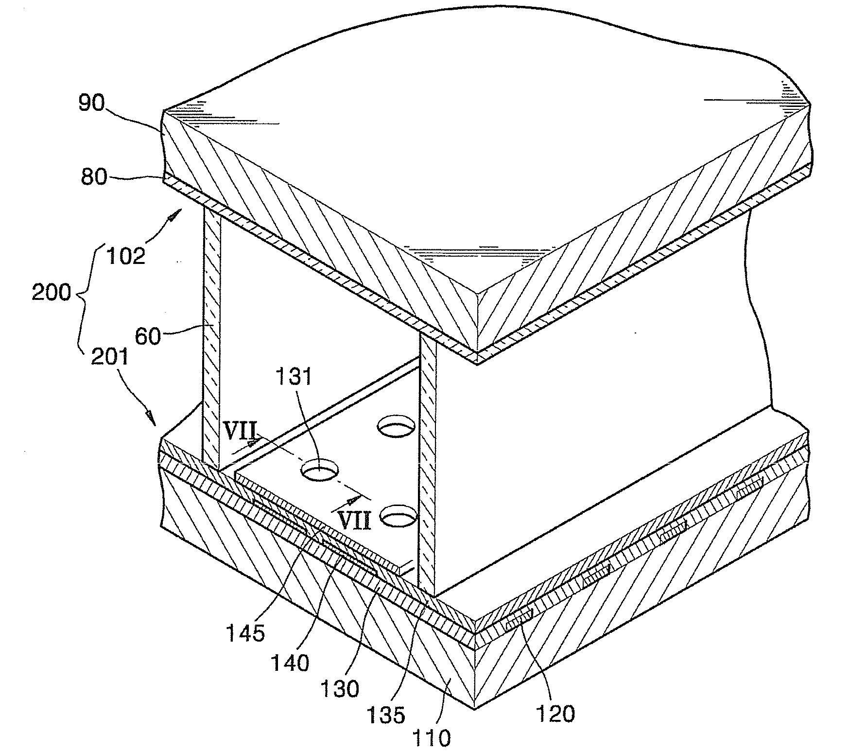
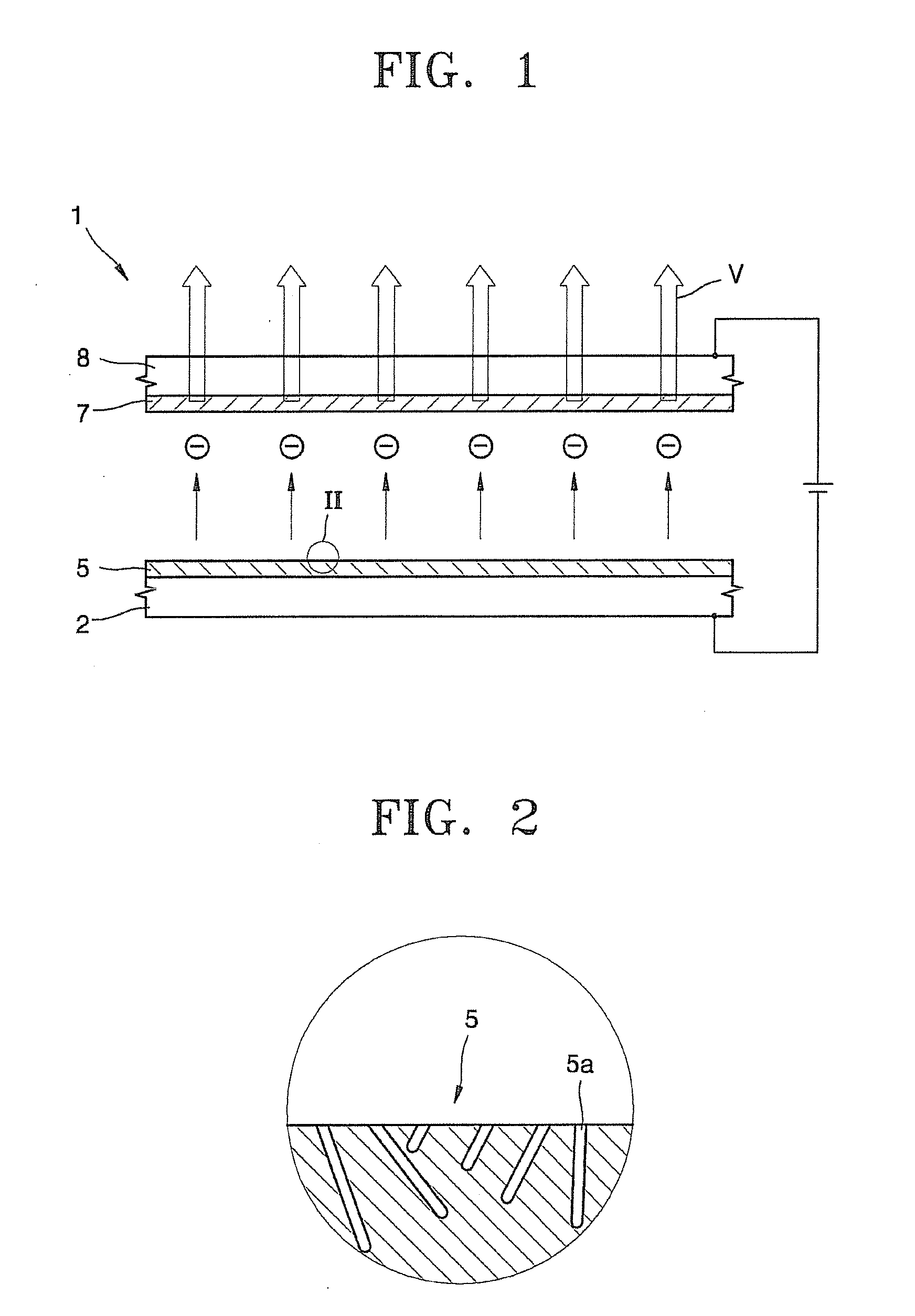
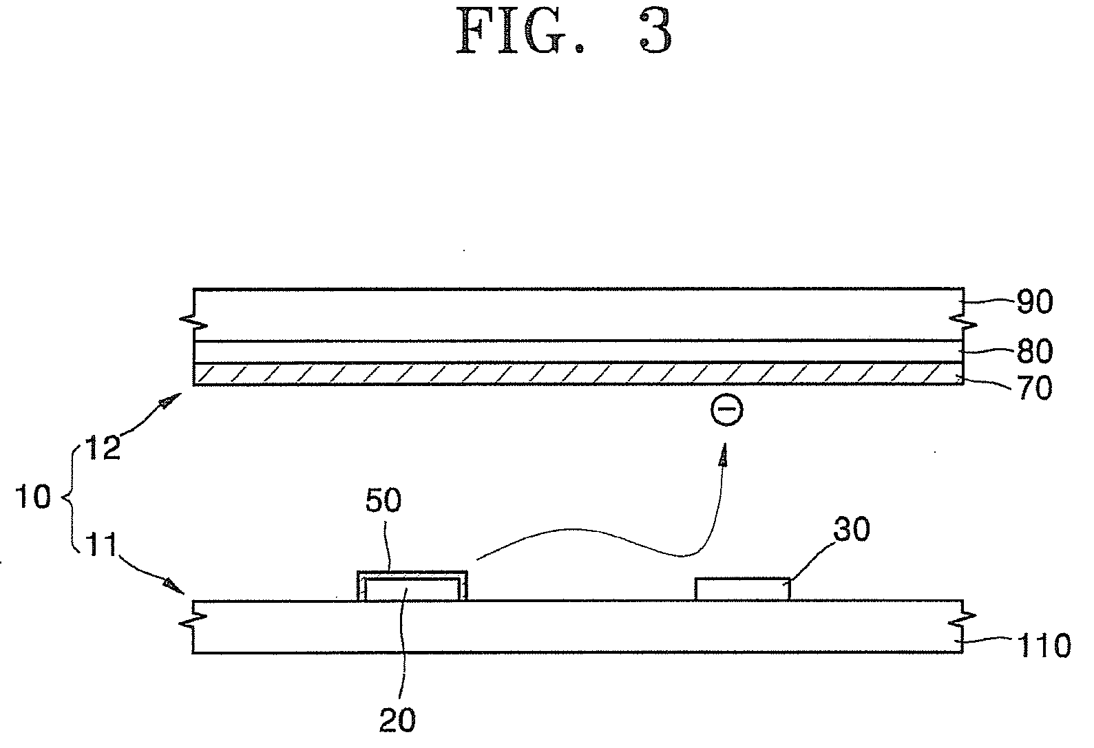
[0030]The method of fabricating an electron emission source according to aspects of the present invention includes forming an electron emission source on a conductive material which may be used as an electrode. Such an electron emission source may be obtained by forming...


PUM


Abstract

A method is provided for fabricating an electron emission source which can attain improved electron emission efficiency and has simplified manufacturing processes. Also provided are an electron emission display device and an electron emission display device fabricated using the method of fabricating an electron emission source. The method includes forming an electrode, forming a carbide compound thin film on the electrode and forming a carbide-induced carbon thin film layer from the carbide compound thin film using an etching gas. The electron emission device and the electron emission display device each include a first electrode, a second electrode disposed to face the first electrode, and a carbide-induced carbon thin film layer formed to be electrically connected to f the first electrode or the second electrode.

Description

CROSS-REFERENCE TO RELATED APPLICATIONS[0001]This application claims the benefit of Korean Application No. 2007-45365, filed May 10, 2007, in the Korean Intellectual Property Office, the disclosure of which is incorporated herein in by reference.BACKGROUND OF THE INVENTION[0002]1. Field of the Invention[0003]Aspects of the present invention relate to electron emission, and more particularly, to a method of fabricating an electron emission source having improved electron emission efficiency, an electron emission device including the electron emission source fabricated using the method, and an electron emission display device including the electron emission device.[0004]2. Description of the Related Art[0005]Generally, electron emission devices use a hot cathode or a cold cathode as an electron emission source. Examples of electron emission devices using a cold cathode include a field emitter array (FEA) type, a surface conduction emitter (SCE) type, a metal insulator metal (MIM) type...

Claims


Application Information

Patent Timeline
Patent Type & Authority Applications(United States)
IPC IPC(8): H01J1/62H01J9/02B05D5/12
CPCH01J1/304H01J9/025H01J29/04H01J31/127H01J63/02H01J63/06H01J2201/30453H01J2201/30484H01J2329/0444H01J2329/0465
Inventor MOON, HEE-SUNGKIM, JAE-MYUNGKIM, YOON-JIN
Owner SAMSUNG SDI CO LTD
Why Eureka
Try Eureka