Matching circuit

a matching circuit and circuit technology, applied in the field of matching circuits, can solve the problems of large circuitry size, difficult to form a multi-band matching circuit by using circuit elements, and large circuitry volume, and achieve the effect of small design

Inactive Publication Date: 2008-11-13
NTT DOCOMO INC
View PDF7 Cites 9 Cited by
  • Summary
  • Abstract
  • Description
  • Claims
  • Application Information

AI Technical Summary

Benefits of technology

[0018]The matching circuit of the present invention is capable of performing impedance matching for each of N frequency bands because the first and third matching parts function as reactance elements having reactance values for each of the frequency bands. Furthermore, because there is a designer's discretion with respect to the configurations of the series reactance circuits of the third matching part, the series reactance circuits are not subject to constraints of the input / output impedances of the circuit element having a frequency characteristic. Therefore, the matching circuit can be designed small by designing the series reactance circuits of the third matching section small.

Problems solved by technology

However, it is not straightforward to form a multiband matching circuit by using circuit elements because each circuit element has a unique frequency characteristic.
If many frequency bands are to be used, a large number of components must be provided, resulting in a large circuitry size.
The increase in the number of components leads not only to a large device size but also to an increase in power consumption in the entire circuitry.
However, it is very difficult to design a delay circuit that is capable of adjusting the amount of delay under the condition that the impedance Z0 should be sustained in each of multiple frequency bands.

Method used


Image

  • Matching circuit
  • Matching circuit
  • Matching circuit

Examples


first embodiment

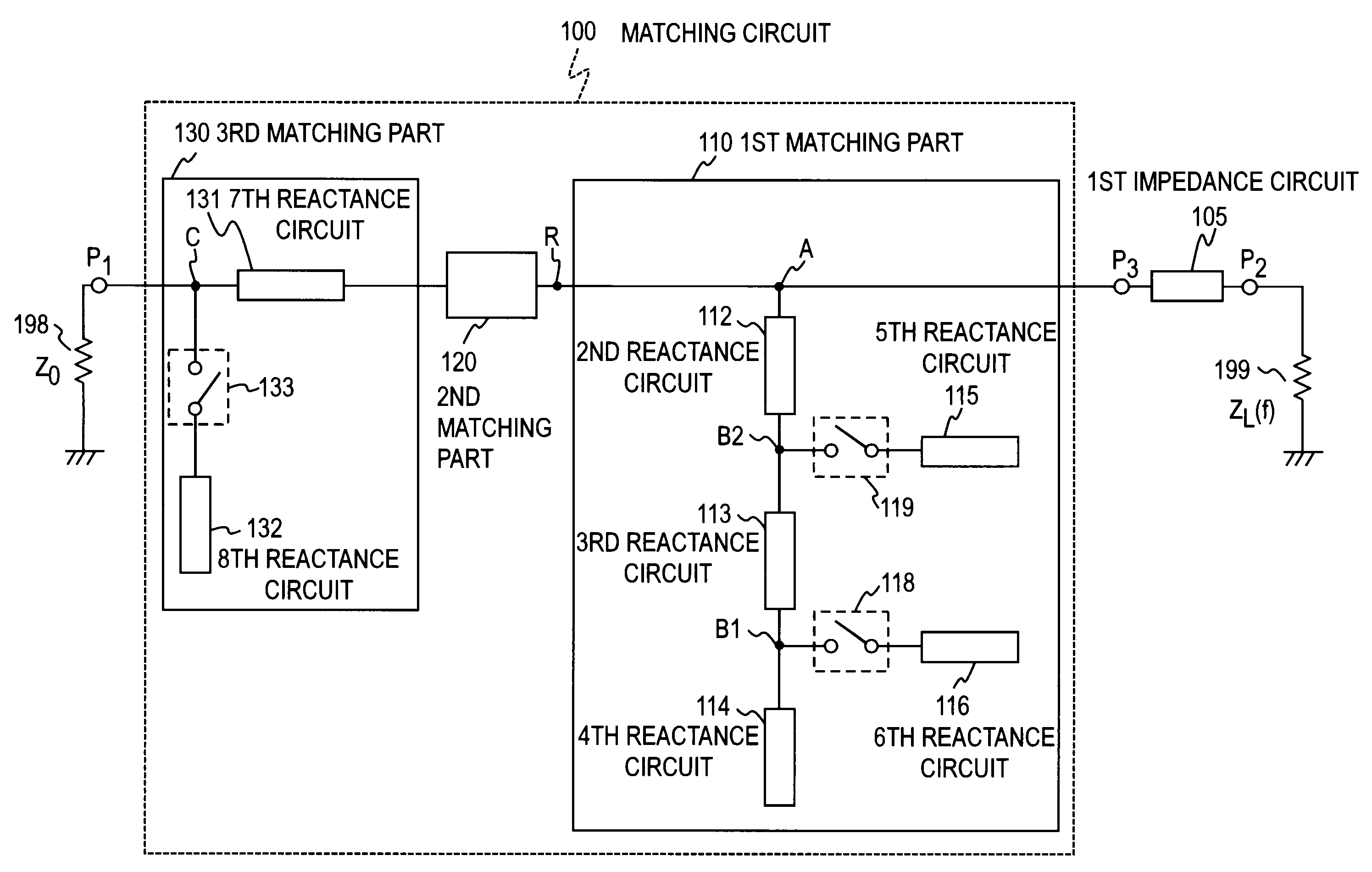
[0038]FIG. 4 shows a matching circuit 100 according to a first embodiment. The matching circuit 100 shown in FIG. 4 operates as a matching circuit for each of signals in two frequency bands with center frequencies f1 and f2 (f1>f2) shown in FIG. 5. The matching circuit 100 is connected in series between port P1 and port P3. The matching circuit 100 includes a first matching part 110, a second matching part 120, and a third matching part 130, which are connected in series in this order. That is, one end of the first matching part 110 is connected to port P3 to which a first impedance circuit 105 is connected. The other end of the first matching part 110 is connected to one end of the second matching part 120. The other end of the second matching part 120 is connected to one end of the third matching part 130. The other end of the third matching part 130 is connected to port P1.

[0039]The first impedance circuit 105 is provided for changing impedance (changing a resistance component is...

second embodiment

[0074]A matching circuit 200 according to a second embodiment is shown in FIG. 9. Like the matching circuit 100 of the first embodiment, the matching circuit 200 shown in FIG. 9 functions as a matching circuit for each of two frequency bands with center frequencies of f1 and f2 (where F1>f2).

[0075]In the first embodiment, the fifth and sixth reactance circuits 115 and 116 are provided in the first matching part 110 for each of the two frequency bands. Accordingly, the desired matching circuit 100 can be configured in spite of the fact that the second reactance circuit 112 has reactance values that is obtained by a single element or circuit constituting the second reactance circuit 112 in each frequency band.

[0076]On the other hand, in the matching circuit 200 of the second embodiment, the number of components of the first matching part 110 is reduced by designing the second reactance circuit 112 so as to have a predetermined reactance value in a certain frequency band.

[0077]For conv...

third embodiment

[0081]Matching circuits that accomplish impedance matching for each of two frequency bands have been shown in the first and second embodiments. In a third embodiment, a matching circuit that accomplishes impedance matching for each of more than two frequency bands will be shown. FIG. 10 shows a matching circuit 300 according to the third embodiment. The matching circuit 300 according to the third embodiment has a configuration similar to that of the matching circuit 100 of the first embodiment. Therefore, the matching circuit 300 will be described in comparison to the matching circuit 100.

[0082]A first matching part 310 of the matching circuit 300 has a configuration in which the fifth and sixth reactance circuits 115 and 116 of the matching circuit 100 are replaced with a fifth and sixth reactance circuits 315 and 316 that are variable reactance circuits whose reactance values can be changed among q kinds of values (where q is an integer greater than or equal to 2). The variable re...


PUM


Abstract

First, second and third matching parts 110, 120, and 130 are connected in series between a circuit element 199 whose impedance has a frequency characteristic and a circuitry 198 having a constant impedance. The second matching part 120 has the capability of converting impedances. The first matching part 110 operates as an element having reactance values according to any of frequency bands selected by exclusive switching between on and off of switches 118, 119 and the third matching part 130 operates as an element having reactance values according to any of the frequency bands selected by switching between on and off of a switch 133, thereby providing matching in each frequency band. A seventh reactance circuit 131 is configured on the basis of an interdependence relation with the configuration of a fifth reactance circuit 115 and an eighth reactance circuit 132.

Description

BACKGROUND OF THE INVENTION[0001]1. Field of the Invention[0002]The present invention relates to a matching circuit used for a circuit element such as an amplifier and, in more specifically, to a matching circuit capable of matching the input / output impedance of a circuit element, such as an amplification device, that has a frequency characteristic to a particular impedance in each of two or more frequency bands.[0003]2. Description of the Related Art[0004]With the diversification of services provided by radio communications, multiband operation of radio devices is required. Among essential devices included in radio devices is a power amplifier. For an efficient amplification, a matching circuit for matching the input / output impedance of an amplification device having a frequency characteristic to the input / output impedance Z0 of peripheral circuitry (hereafter referred to as the system impedance Z0), namely a multiband matching circuit, is required.[0005]FIG. 1 shows an example of ...

Claims


Application Information

Patent Timeline
Patent Type & Authority Applications(United States)
IPC IPC(8): H03H7/38
CPCH03F1/56H03F3/193H03F3/601H03F2200/111H03F2200/387H03F2200/423H03F2200/451H03H7/38H03F1/08
Inventor FUKUDA, ATSUSHIOKAZAKI, HIROSHINARAHASHI, SHOICHI
Owner NTT DOCOMO INC
Why Eureka
Try Eureka