Method of growing gan crystal on silicon substrate, and light emitting device and method of manufacturing thereof

a technology of gan crystal and silicon substrate, which is applied in the direction of semiconductor/solid-state device manufacturing, semiconductor devices, electrical devices, etc., can solve the problems of reducing manufacturing processes, gan light emitting devices may not use silicon substrates, and the use of higher electrical conductivity and thermal conductivity of silicon substrates, so as to reduce manufacturing costs and reduce manufacturing costs , the effect of cost reduction

Active Publication Date: 2008-11-20
SAMSUNG CORNING PRECISION MATERIALS CO LTD
View PDF8 Cites 63 Cited by
  • Summary
  • Abstract
  • Description
  • Claims
  • Application Information

AI Technical Summary

Benefits of technology

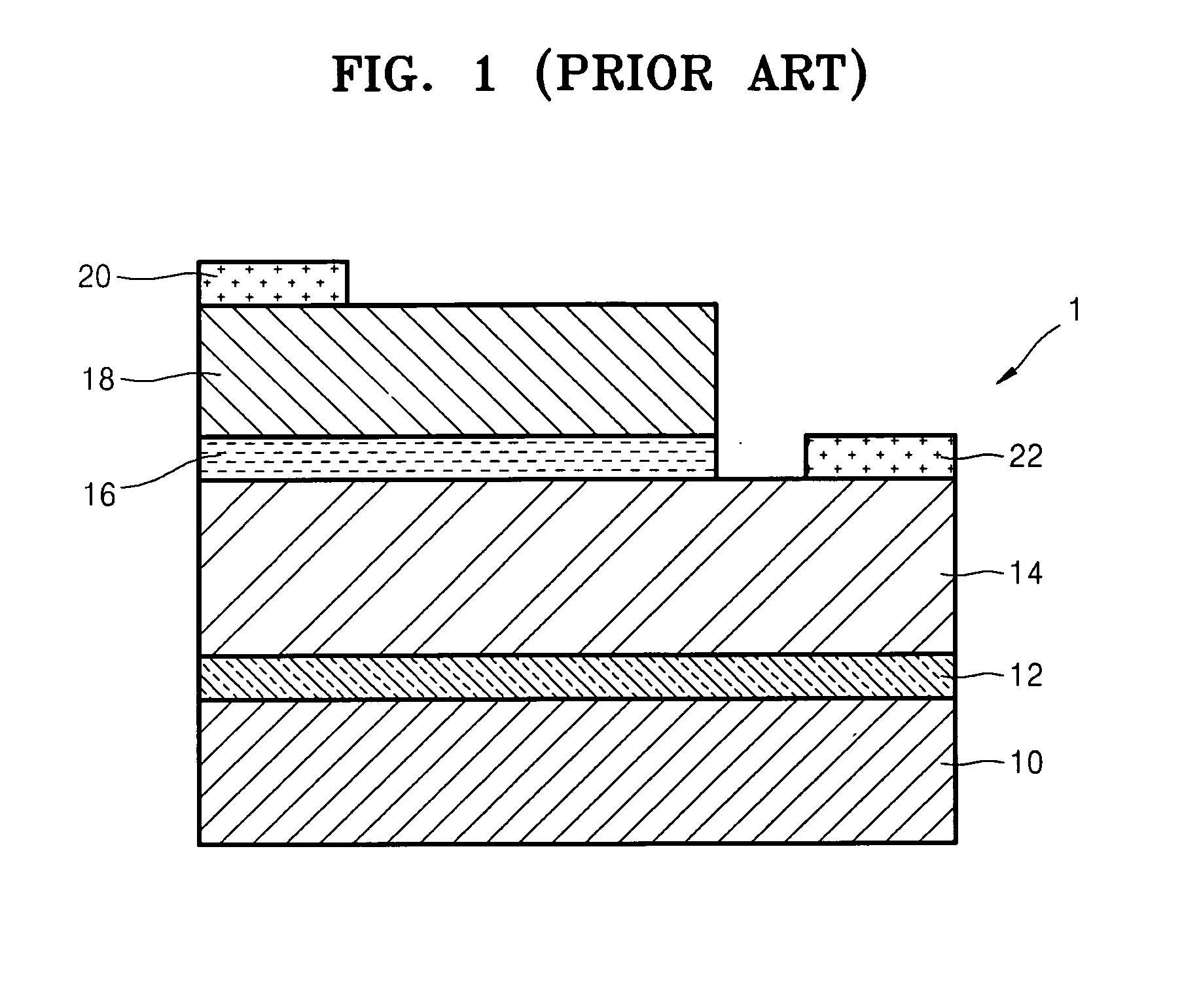
[0007]In an example embodiment of the light emitting device 1 having the above structure, if the sapphire substrate 10 can be replaced by a silicon substrate, manufacturing costs may be reduced since the cost of the silicon substrate may be less than the sapphire substrate 10, the SiC substrate, or other like substrate. A larger silicon substrate or other like substrate may be used in the above light emitting device 1, and this may also achieve cost reduction. Also, due to the higher electrical conductivity of the silicon substrate or other like substrate, an electrode may be formed on a lower surface of the silicon substrate, and this may result in reduced manufacturing processes.

Problems solved by technology

Also, due to the higher electrical conductivity of the silicon substrate or other like substrate, an electrode may be formed on a lower surface of the silicon substrate, and this may result in reduced manufacturing processes.
However, a GaN light emitting device may not use a silicon substrate because thermal expansion may cause severe cracks to form between the silicon substrate and the GaN thin film layer.
However, the higher electrical conductivity and higher thermal conductivity of the silicon substrate may not be utilized because the AlN layer has a lower electrical conductivity.

Method used


Image

  • Method of growing gan crystal on silicon substrate, and light emitting device and method of manufacturing thereof
  • Method of growing gan crystal on silicon substrate, and light emitting device and method of manufacturing thereof
  • Method of growing gan crystal on silicon substrate, and light emitting device and method of manufacturing thereof

Examples


Embodiment Construction

[0023]Detailed example embodiments are disclosed herein. However, specific structural and functional details disclosed herein are merely representative for purposes of describing example embodiments. Example embodiments may, however, be embodied in many alternate forms and should not be construed as limited to only the embodiments set forth herein.

[0024]Accordingly, while example embodiments are capable of various modifications and alternative forms, embodiments thereof are shown by way of example in the drawings and will herein be described in detail. It should be understood, however, that there is no intent to limit example embodiments to the particular forms disclosed, but to the contrary, example embodiments are to cover all modifications, equivalents, and alternatives falling within the scope of example embodiments. Like numbers refer to like elements throughout the description of the figures.

[0025]It will be understood that, although the terms first, second, etc. may be used h...


PUM

PropertyMeasurementUnit
thicknessaaaaaaaaaa
thicknessaaaaaaaaaa
thicknessaaaaaaaaaa

Abstract

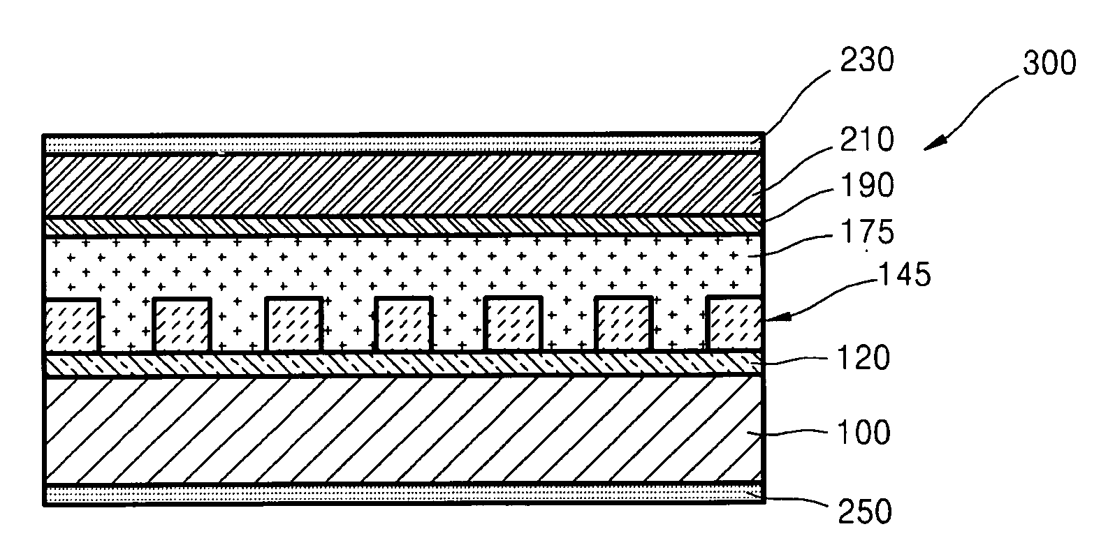
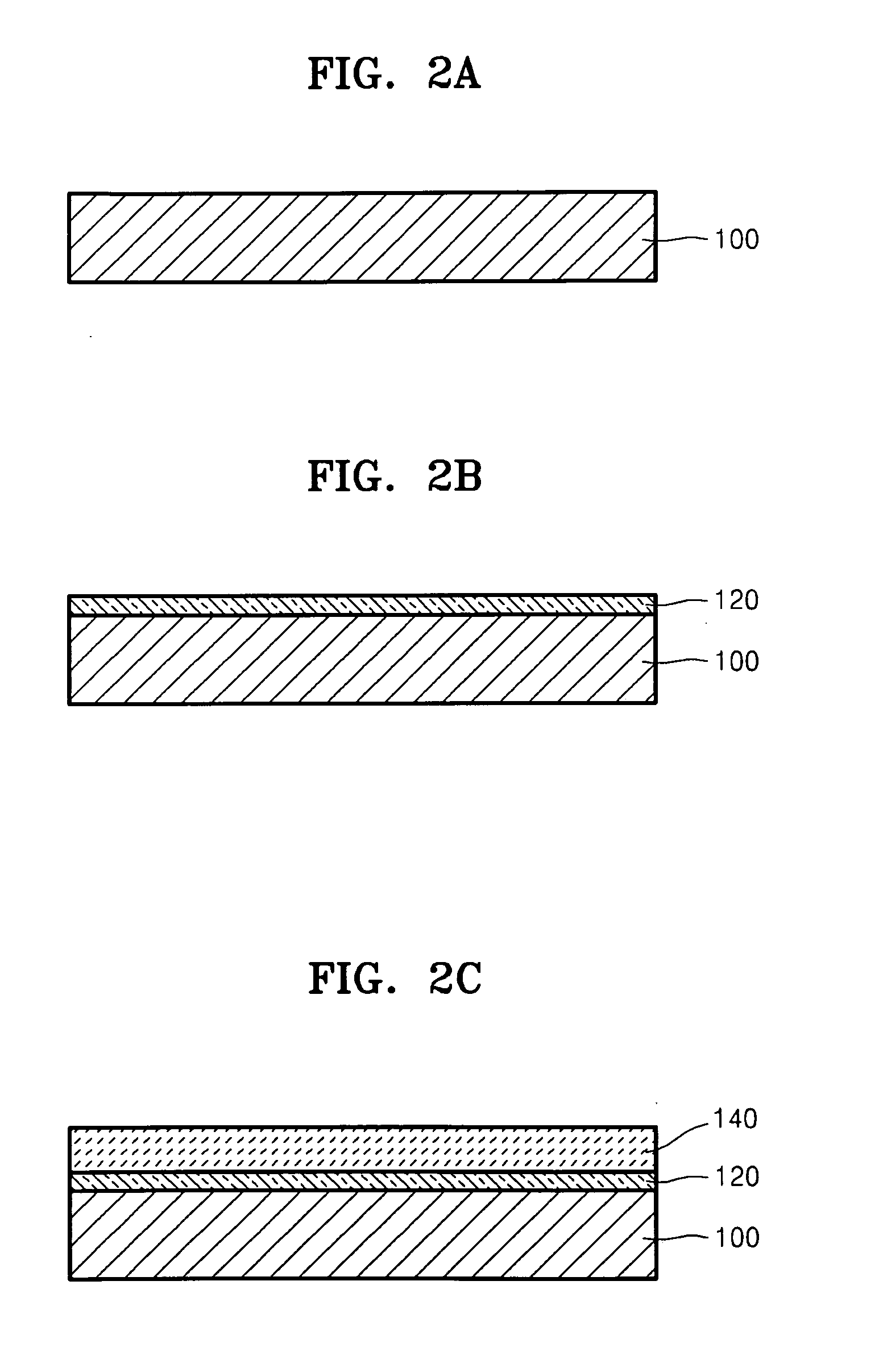
Example embodiments are directed to a method of growing GaN single crystals on a silicon substrate, a method of manufacturing a GaN-based light emitting device using the silicon substrate, and a GaN-based light emitting device. The method of growing the GaN single crystals may include forming a buffer layer including a TiN group material or other like material on a silicon substrate, forming a nano-pattern including silicon oxide on the buffer layer, and growing GaN single crystals on the buffer layer and the nano-pattern.

Description

FOREIGN PRIORITY STATEMENT[0001]This application claims priority under 35 U.S.C. § 119 to Korean Patent Application No. 10-2007-0048309, filed on May 17, 2007 in the Korean Intellectual Property Office, the entire contents of which are incorporated herein by reference.BACKGROUND[0002]1. Field[0003]Example embodiments are directed to a method of growing GaN single crystals on a silicon substrate, a method of manufacturing a GaN-based light emitting device using the silicon substrate, and a GaN-based light emitting device manufactured using the silicon substrate. Example embodiments include a method of growing GaN single crystals using a TiN group metal nitride as a buffer layer, a method of manufacturing a GaN-based light emitting device using a silicon substrate, and a GaN-based light emitting device manufactured using a silicon substrate.[0004]2. Description of the Related Art[0005]Nitride group semiconductors such as GaN may be used in light emitting devices, and examples of such ...

Claims


Application Information

Patent Timeline
Patent Type & Authority Applications(United States)
IPC IPC(8): H01L33/00H01L21/205H01L33/12H01L33/20
CPCH01L21/02381H01L21/02488H01L21/02491H01L21/0254H01L33/20H01L21/02645H01L33/007H01L33/12H01L21/02639
Inventor PARK, SUNG-SOOLEE, JUNE-KEY
Owner SAMSUNG CORNING PRECISION MATERIALS CO LTD
Why Eureka
Try Eureka