Semiconductor device having tipless epitaxial source/drain regions

Active Publication Date: 2008-11-20
INTEL CORP
View PDF15 Cites 117 Cited by
  • Summary
  • Abstract
  • Description
  • Claims
  • Application Information

AI Technical Summary

Problems solved by technology

One drawback to this approach is that gate isolation spacers 108 are required to inhibit undesirable material growth on gate electrode 106 during epi

Method used


Image

  • Semiconductor device having tipless epitaxial source/drain regions
  • Semiconductor device having tipless epitaxial source/drain regions
  • Semiconductor device having tipless epitaxial source/drain regions

Examples


Embodiment Construction

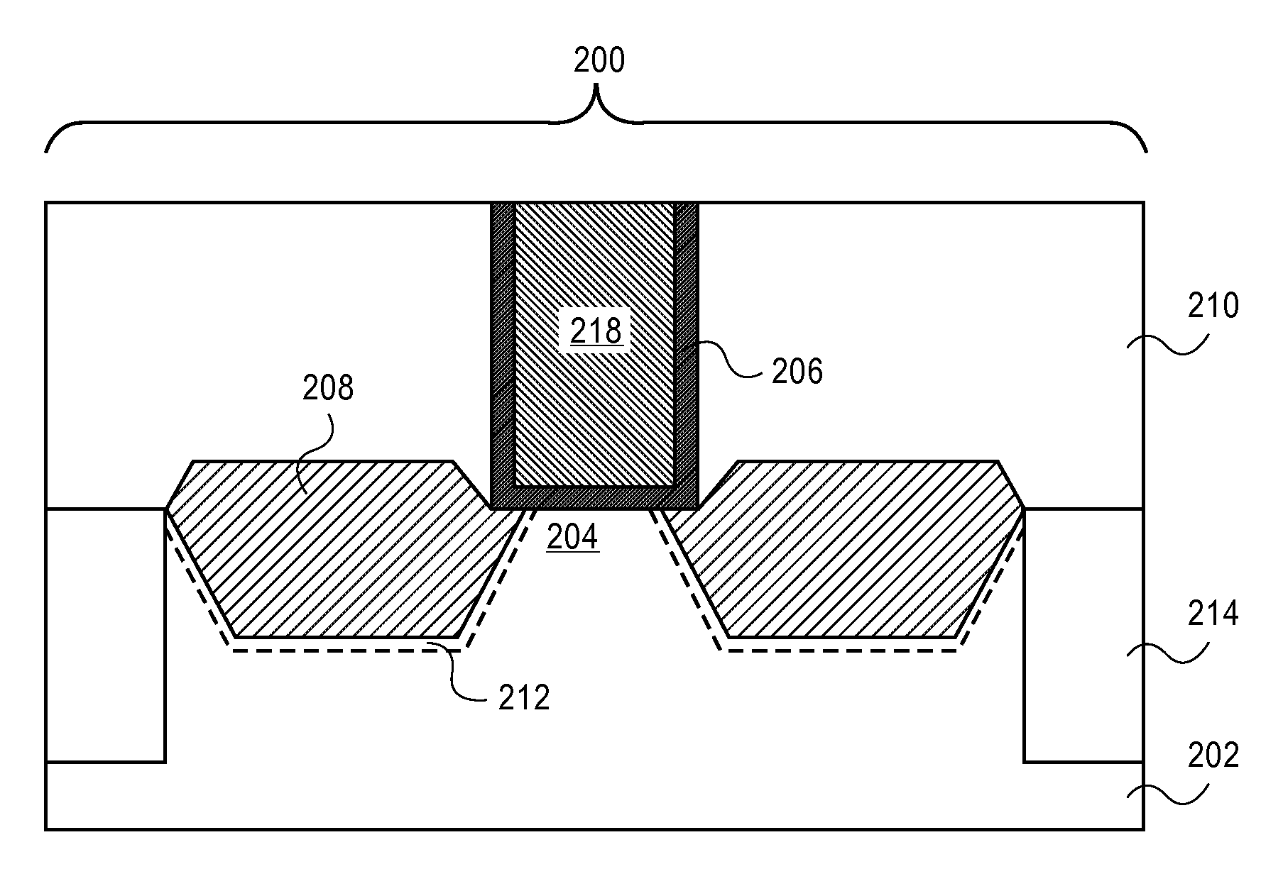
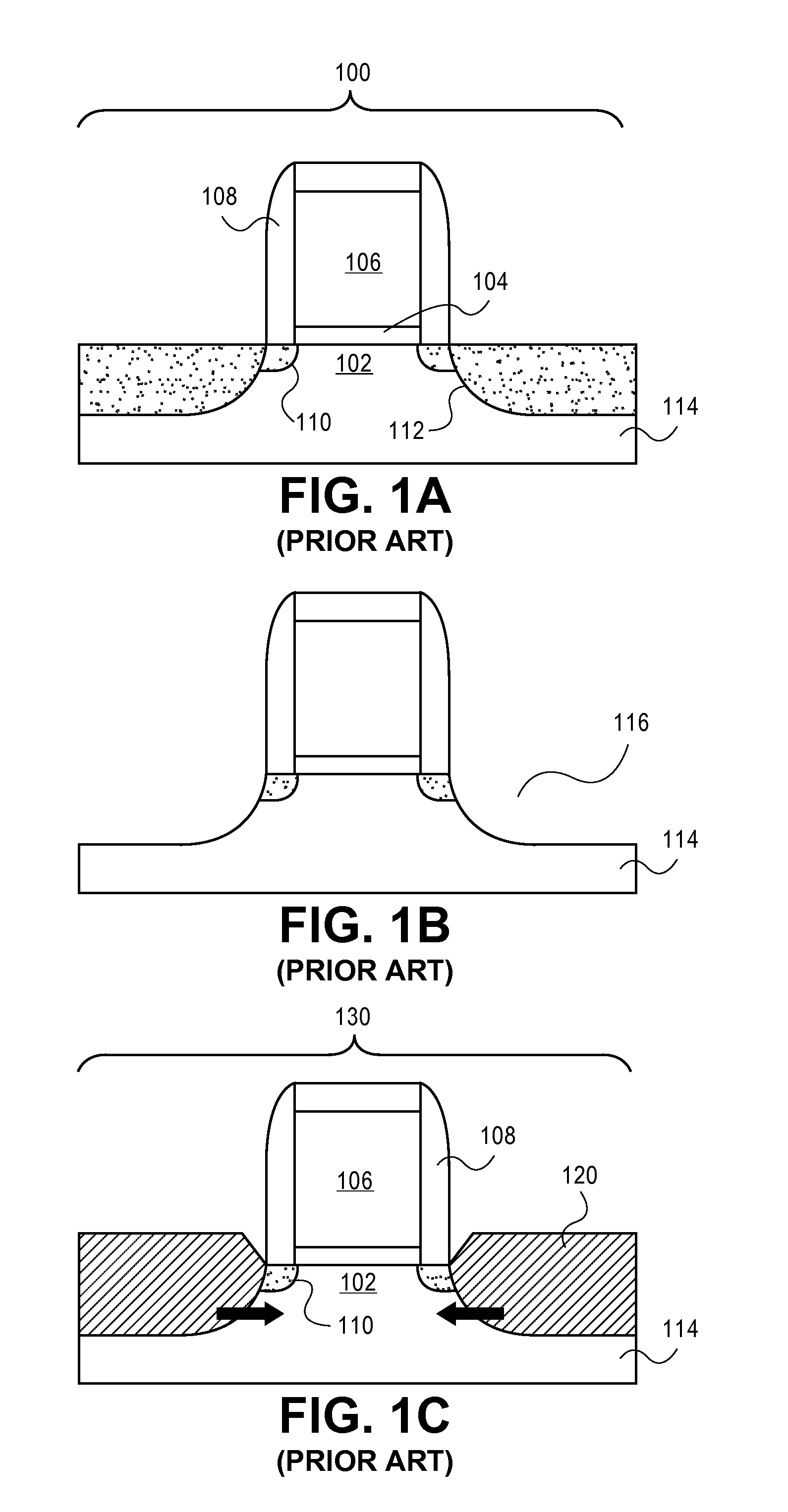
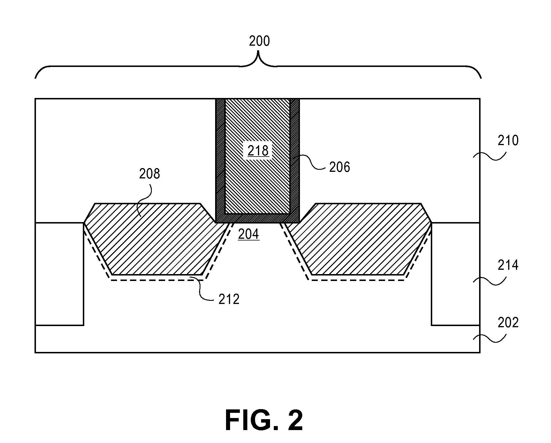
[0014]A semiconductor device having tipless epitaxial source / drain regions and a method for its formation are described. In the following description, numerous specific details are set forth, such as specific dimensions and chemical regimes, in order to provide a thorough understanding of the present invention. It will be apparent to one skilled in the art that the present invention may be practiced without these specific details. In other instances, well-known processing steps such as patterning steps or wet chemical cleans are not described in detail in order to not unnecessarily obscure the present invention. Furthermore, it is to be understood that the various embodiments shown in the Figures are illustrative representations and are not necessarily drawn to scale.

[0015]Disclosed herein are a semiconductor device having tipless epitaxial source / drain regions and a method to form such a device. In an embodiment, the semiconductor device comprises a gate stack on a substrate. The g...


PUM


Abstract

A semiconductor device having tipless epitaxial source/drain regions and a method for its formation are described. In an embodiment, the semiconductor device comprises a gate stack on a substrate. The gate stack is comprised of a gate electrode above a gate dielectric layer and is above a channel region in the substrate. The semiconductor device also comprises a pair of source/drain regions in the substrate on either side of the channel region. The pair of source/drain regions is in direct contact with the gate dielectric layer and the lattice constant of the pair of source/drain regions is different than the lattice constant of the channel region. In one embodiment, the semiconductor device is formed by using a dielectric gate stack placeholder.

Description

BACKGROUND OF THE INVENTION[0001]1) Field of the Invention[0002]The invention is in the field of Semiconductor Devices.[0003]2) Description of Related Art[0004]For the past several years, the performance of semiconductor devices, such as Metal Oxide Semiconductor Field-Effect Transistors (MOS-FETs), has been greatly enhanced by the incorporation of strained channel regions into the active portions of a semiconductor substrate, e.g. the use of compressively strained silicon channel regions to enhance hole mobility in P-type Metal Oxide Semiconductor Field-Effect Transistors (PMOS-FETs). The presence of such strained channel regions may greatly enhance the rate at which charge migrates in a channel when a semiconductor device is in an ON state.[0005]FIGS. 1A-C illustrate cross-sectional views representing a typical process flow for forming strain-inducing source / drain regions in a PMOS-FET, in accordance with the prior art. Referring to FIG. 1A, a non-strained PMOS-FET 100 is first fo...

Claims


Application Information

Patent Timeline
IPC IPC(8): H01L29/778H01L21/336H01L29/76
CPCH01L29/045H01L29/165H01L29/66545H01L29/66628H01L29/785H01L29/66795H01L29/7834H01L29/7848H01L29/66636H01L29/41725H01L29/7378H01L21/845H01L29/0653H01L29/0847H01L29/161H01L29/167H01L29/7851
Inventor BOHR, MARK T.
Owner INTEL CORP
Why Eureka
Try Eureka