Semiconductor module and method for manufacturing semiconductor module

a semiconductor module and semiconductor technology, applied in the direction of semiconductor devices, semiconductor/solid-state device details, electrical apparatus, etc., can solve the problems of inability to obtain adequate cooling effect, damage to insulating sheet 104/b>, and inability to reduce the weight and size of semiconductor modules, etc., to achieve low cost, small size, and light weight

Active Publication Date: 2008-11-20
FUJI ELECTRIC CO LTD
View PDF2 Cites 15 Cited by
  • Summary
  • Abstract
  • Description
  • Claims
  • Application Information

AI Technical Summary

Benefits of technology

[0028]By this means, a semiconductor module and a method for manufacturing a semiconductor module can be made such that the semiconductor module mounted with power semiconductor devices is light in weight, small in size, and low in cost, has an adequate cooling effect, and can be mounted with high-power semiconductor devices.

Problems solved by technology

However, such a semiconductor module 100 employs a thick metal base plate 101 as a foundation, so that the weight and size of the semiconductor module cannot be decreased.
As a result, the insulating sheet 104 is damaged.
As a result, there has been a problem that an adequate cooling effect cannot be obtained.
For this reason, there has been a problem that high-power semiconductor devices could not be incorporated into such semiconductor modules 200.

Method used


Image

  • Semiconductor module and method for manufacturing semiconductor module
  • Semiconductor module and method for manufacturing semiconductor module
  • Semiconductor module and method for manufacturing semiconductor module

Examples


Embodiment Construction

[0037]Below, the invention is explained in detail, referring to the drawings.

[0038]First, the configuration of a semiconductor module is explained.

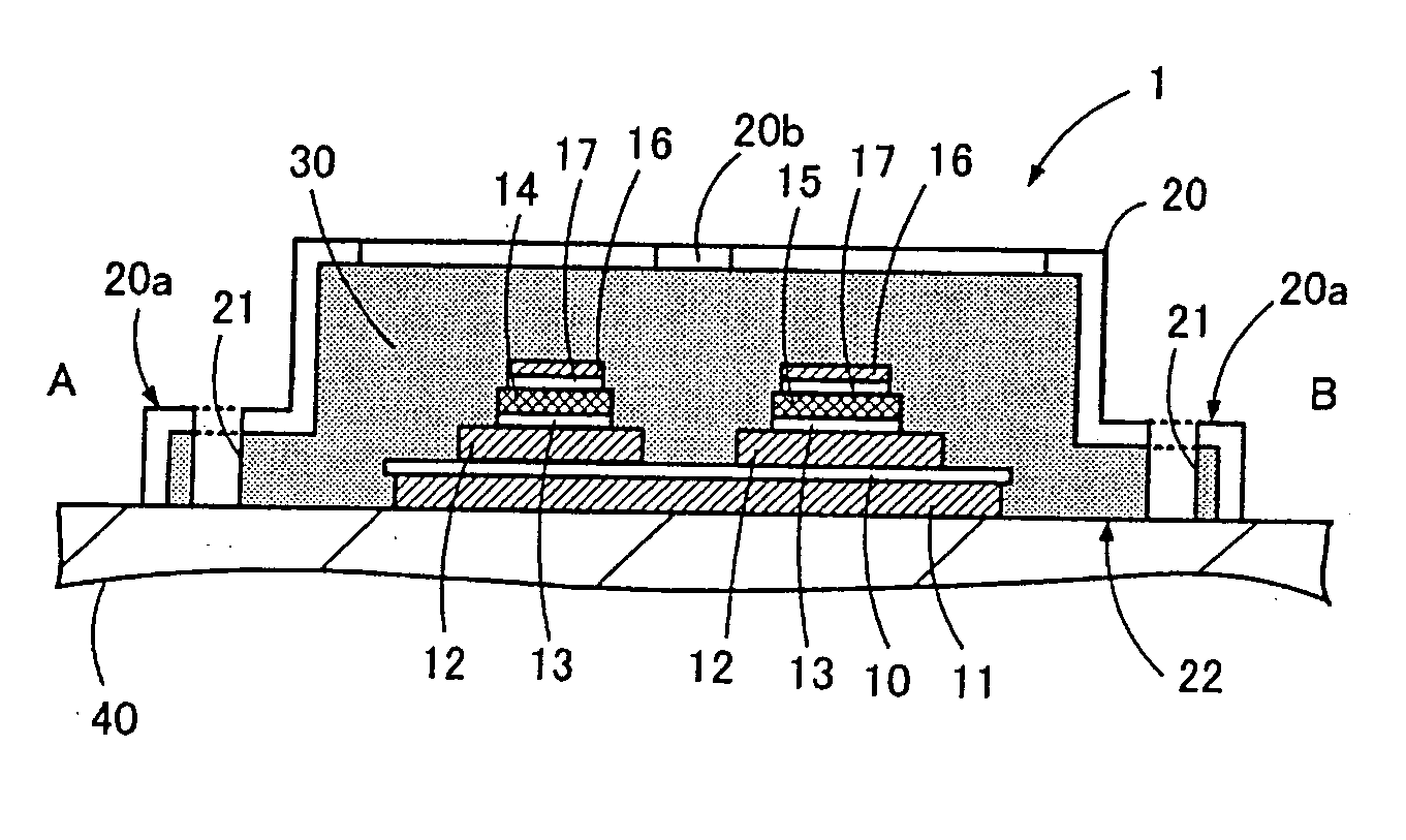
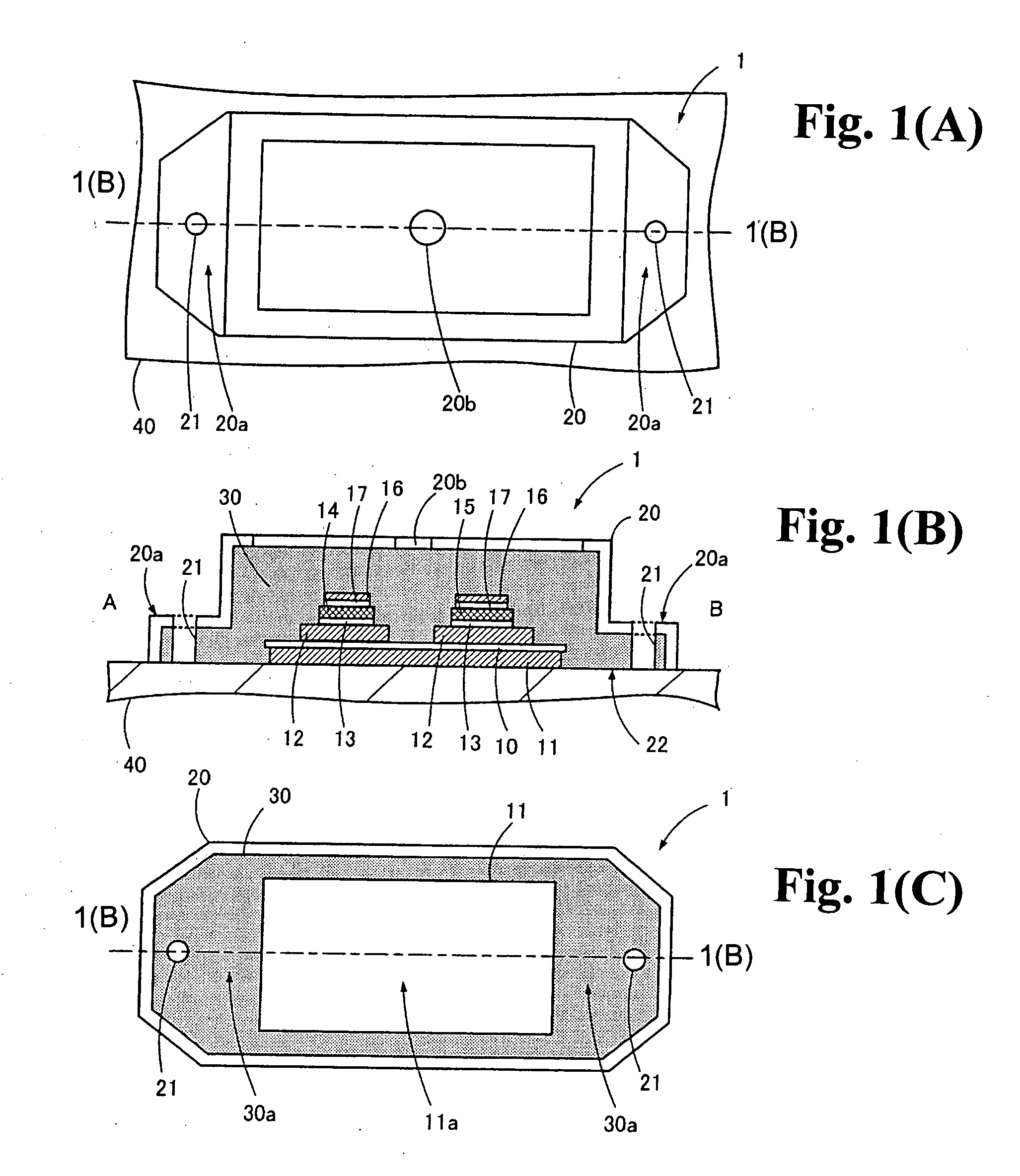
[0039]FIGS. 1(A), 1(B), 1(C) are schematic diagrams of principal portions, explaining the configuration of a semiconductor module. Here, in FIG. 1(A), a schematic top view of principal portions of a semiconductor module 1 is shown, and in FIG. 1(B), a schematic diagram of a cross-section of principal portions of the semiconductor module 1 is shown. In FIG. 1(C), a schematic bottom view of principal portions of the semiconductor module 1 is shown.

[0040]Also, in FIG. 1(B), a cross-sectional view taken along a line 1(B)-1(B) in FIGS. 1(A) and 1(C) is shown. In FIGS. 1(A), 1(B), a state is shown in which a cooling member 40 (cooling fins), which is the external mounting member, is mounted to the lower face of the semiconductor module 1. In FIG. 1(C), however, the cooling member 40 is not shown in order to clearly display the lower face of the...


PUM


Abstract

A semiconductor module includes a first metal foil; an insulating sheet mounted on a top surface of the first metal foil; at least one second metal foil mounted on a top surface of the insulating sheet; at least one semiconductor device mounted on the second metal foil; and a resin case for surrounding the first metal foil, insulating sheet, second metal foil, and semiconductor device. A bottom end of a peripheral wall of the resin case is located above a bottom surface of the first metal foil. A resin is provided inside the resin case to fill the inside of the resin case. The bottom surface of the first metal foil and the resin form a flat bottom surface so that the flat bottom surface contacts an external mounting member.

Description

BACKGROUND OF THE INVENTION AND RELATED ART STATEMENT[0001]This invention relates to a semiconductor module and a method for manufacturing a semiconductor module, and in particular relates to a semiconductor module mounted with a power semiconductor device, and a method for manufacturing such a semiconductor module.[0002]In inverter devices, uninterruptible power supply devices, machining equipments, industrial robots, and other equipments, semiconductor modules, which are independent of the main unit of the equipment, are employed.[0003]As the construction of such semiconductor modules, generally, a metal base plate of prescribed thickness is used as a foundation, and a package mounted with power semiconductor devices is provided on the metal base plate (see for example Japanese Unexamined Patent Publication No. 2003-289130). For example, FIG. 7 is a schematic diagram of a semiconductor module employing a metal base plate as a foundation.[0004]This semiconductor module 100 employs ...

Claims


Application Information

Patent Timeline
Patent Type & Authority Applications(United States)
IPC IPC(8): H01L23/485H01L21/60
CPCH01L23/3121H01L25/072H01L2924/3511H01L2924/13091H01L2224/32225H01L2924/1305H01L2924/13055H01L2924/00
Inventor HORIO, MASAFUMINISHIZAWA, TATSUOMOCHIZUKI, EIJIMARUYAMA, RIKIHIRO
Owner FUJI ELECTRIC CO LTD
Why Eureka
Try Eureka