Active matrix organic light emitting diode display

a technology of organic light and diodes, applied in the field of flat panel displays, can solve the problems that the wide dynamic range dimming (e.g., >2000:1) cannot be achieved with suitable uniformity, and achieve the effect of maintaining color balance, maintaining luminance and chromaticity of the display, and low gray-levels

Active Publication Date: 2008-11-20
HONEYWELL INT INC
View PDF13 Cites 24 Cited by
  • Summary
  • Abstract
  • Description
  • Claims
  • Application Information

AI Technical Summary

Benefits of technology

[0013]The present invention provides an improved AM OLED pixel circuit and method of wide dynamic range dimming for AM OLED displays that maintains color balance throughout the dimming range, and also maintains the uniformity of the luminance and chromaticity of the display at low gray-levels as the display is dimmed to lower luminance values. As such, the present invention enables AM OLED displays to meet the stringent color / dimming specifications required for existing and future avionics, cockpit, and hand-held military device display applications. Essentially, the present invention provides an improved AM OLED pixel circuit and method of dynamic range dimming that uses Pulse Width Modulation (PWM) of the OLED pixel current to achieve the desired display luminance (brightness).
[0014]Two example embodiments of the invention are provided for externally (e.g., outside an AM OLED glass display) PW modulating the common cathode voltage (VK) or common power supply voltage (VDD) so as to modulate the OLED current in order to achieve the desired display luminance. Three additional example embodiments of the invention are provided that incorporate additional transistor switches in the pixel circuit in order to modulate the OLED current during the frame time. Unlike the conventional methods, the three additional (internal) example embodiments allow modulation of each row of pixels sequentially during the frame time, which eliminates any propensity for display flicker. Thus, by PW modulating the OLED current, in combination with data voltage (or current) modulation, the present invention achieves wide dynamic range dimming while maintaining the color balance and the luminance and chromaticity uniformity required over the surface of the display involved.

Problems solved by technology

However, as discussed earlier, it can be seen from FIG. 1 that a significant problem with these conventional methods of adjusting the luminance of an AM OLED display is that because the dimming is performed by changing the data voltage (or current), or by changing the power supply (VDD and / or VK) voltages to adjust the grayscale, wide dynamic range dimming (e.g., >2000:1) cannot be achieved with suitable uniformity.

Method used


Image

  • Active matrix organic light emitting diode display
  • Active matrix organic light emitting diode display
  • Active matrix organic light emitting diode display

Examples


first embodiment

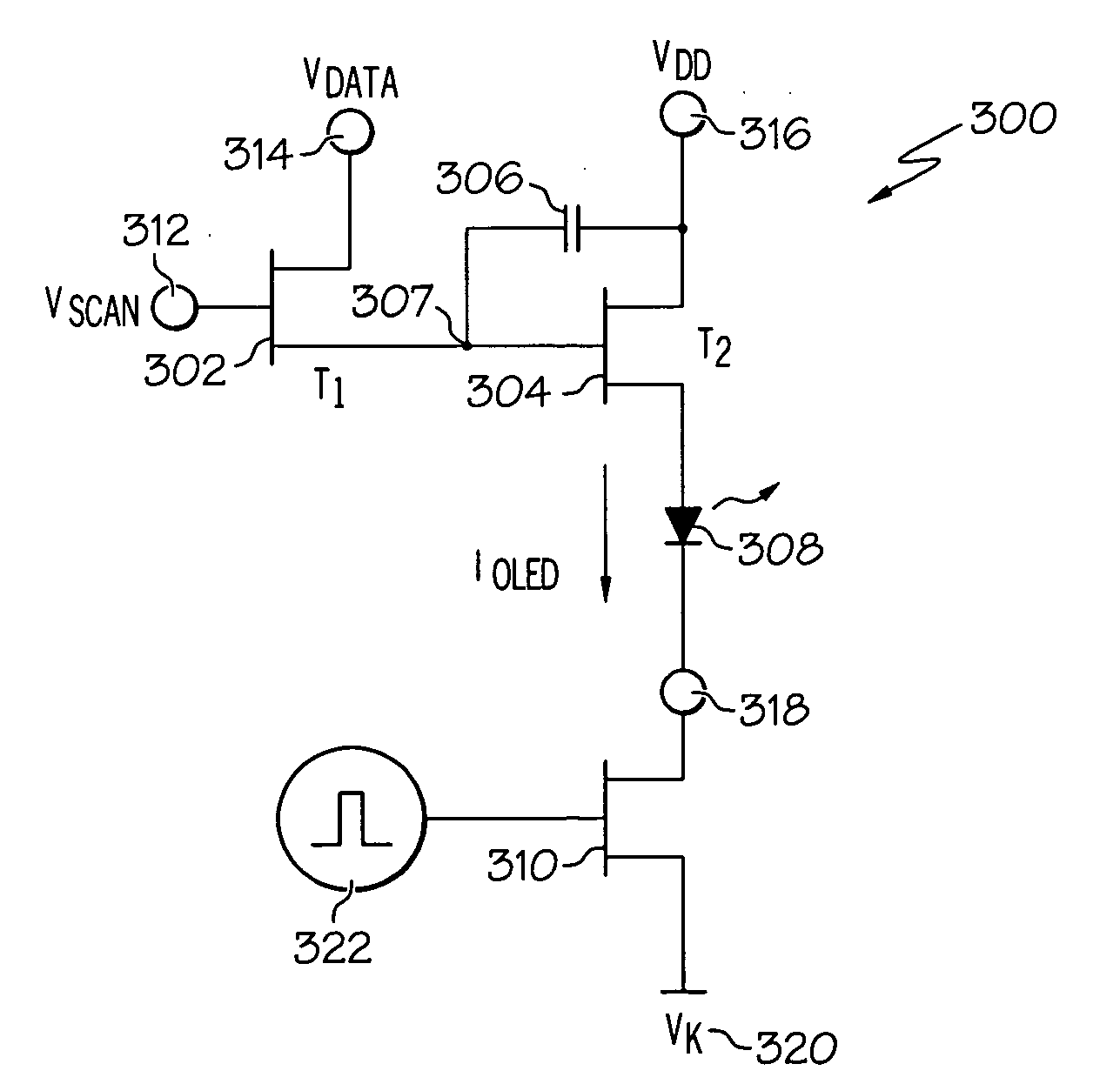
[0025]FIG. 3 depicts an electrical schematic diagram of an example AM OLED sub-pixel circuit 300, which can be used to implement the present invention. As such, AM OLED sub-pixel circuit 300 can be used in a preferred method for dynamically dimming an AM OLED display using, for example, an external (to the display) PWM scheme. Referring now to FIG. 3, AM OLED sub-pixel circuit 300 includes a first TFT 302, a second TFT 304, a storage capacitor 306, an OLED pixel 308, and a transistor 310, represented here by a Field Effect Transistor (FET). As shown, transistor 302 is a scan transistor, and transistor 304 is a drive transistor. The gate terminal 312 of the scan transistor 302 is connected to the row (scan / row enable) address bus of the display involved, and the drain terminal 314 of scan transistor 302 is connected to the column (data) address bus of the display. The source of scan transistor 302 is connected to the node 307 at the storage capacitor 306 and the gate terminal of the ...

second embodiment

[0029]FIG. 4 depicts an electrical schematic diagram of an example AM OLED sub-pixel circuit 400, which can be used to implement the present invention. As such, AM OLED sub-pixel circuit 400 can be used in a preferred method for dynamically dimming an AM OLED display using, for example, an external (to the display) PWM scheme. Referring now to FIG. 4, AM OLED sub-pixel circuit 400 includes a first TFT 402, a storage capacitor 404, a second TFT 408, an OLED pixel 410, and a transistor 406 represented here by a P-channel FET. In this case, an external (to the display involved) transistor 406 can be used to PW modulate the positive power supply, VDD 418, of the OLED pixel 410, in order to turn “off” the voltage across the OLED pixels (e.g., OLED pixel 410) associated with the common power supply voltage, VDD 418, and thus to control the brightness of the display. Also, in this case, the reference voltage, VSC 416, for storage capacitor 404, can be removed from the VDD line to prevent c...

third embodiment

[0033]FIG. 5 depicts an electrical schematic diagram of an example AM OLED sub-pixel circuit 500, which can be used to implement the present invention. As such, AM OLED sub-pixel circuit 500 can be used in a preferred method for dynamically dimming an AM OLED display using, for example, an internal (to the display) PWM scheme. Referring now to FIG. 5, AM OLED sub-pixel circuit 500 includes a first TFT 502, a storage capacitor 504, a second TFT 506, a third TFT 508, and an OLED pixel 510. In this case, a third TFT 508 (internal to the display involved) can be used at each sub-pixel in the display to PW modulate the current, IOLED 518, of the OLED pixel 510, in order to turn “off” the OLED pixel (e.g., OLED pixel 510) so that it does not emit light, and thus control the brightness of the overall display.

[0034]As shown, for this example embodiment, transistor 502 is a scan transistor, and transistor 506 is a drive transistor. The gate terminal 512 of the scan transistor 502 is connecte...


PUM


Abstract

An improved AM OLED pixel circuit and method of wide dynamic range dimming for AM OLED displays are disclosed that maintain color balance throughout the dimming range, and also maintain the uniformity of the luminance and chromaticity of the display at low gray-levels as the display is dimmed to lower luminance values. As such, AM OLED displays can meet the stringent color / dimming specifications required for existing and future avionics, cockpit, and hand-held military device display applications. Essentially, the OLED pixel circuit and method of dimming that are disclosed use Pulse Width Modulation (PWM) of the OLED pixel current to achieve the desired display luminance. Two example circuits are disclosed that externally PW modulate the common cathode voltage or common power supply voltage to modulate the OLED current in order to achieve the desired display luminance. Three example circuits are disclosed that incorporate additional transistor switches in the pixel circuit to modulate the OLED current during the frame time. By PWM of the OLED current, in combination with data voltage (or current) modulation, wide dynamic range dimming can be achieved while maintaining the color balance and the luminance and chromaticity uniformity required over the surface of the display involved.

Description

CROSS REFERENCE TO RELATED APPLICATION[0001]This application is a divisional of Ser. No. 11 / 043,657 filed on Jan. 26, 2005.BACKGROUND OF THE INVENTION[0002]1. Technical Field[0003]The present invention relates generally to the field of flat panel displays, and more specifically, but not exclusively, to an improved Active Matrix Organic Light Emitting Diode (AM OLED) display and method of wide dynamic range dimming in such a display for commercial and military applications, such as, for example, cockpit displays, avionics displays, or hand-held military communication device displays.[0004]2. Description of Related Art[0005]AM OLED displays are an emerging flat panel display technology, which has already produced such new products as passive matrix-addressed displays that can be used for cell-phones and automobile audio systems. AM OLED displays are most likely to replace backlit AM Liquid Crystal Displays (LCDs) because AM OLED displays are more power efficient, rugged, weigh less, c...

Claims


Application Information

Patent Timeline
Patent Type & Authority Applications(United States)
IPC IPC(8): G09G3/30
CPCG09G3/3233G09G2300/0842G09G2320/0233G09G2320/0606G09G2320/0626G09G2300/0861G09G3/20G09G3/30G09G3/32H05B33/12G09G2310/06
Inventor SARMA, KALLURI R.ROUSH, JERRY A.SCHMIDT, JOHN
Owner HONEYWELL INT INC
Why Eureka
Try Eureka