Liquid crystal display device and manufacturing method thereof

a liquid crystal display device and manufacturing method technology, applied in non-linear optics, instruments, optics, etc., can solve the problems of high risk of impurity penetration into the liquid crystal drop method, the impurity penetration of the liquid crystal layer is at the risk of being penetrated by the outside, etc., to prevent the diffusion of impurity from the conductor into the liquid crystal layer, reduce the display defect of the liquid crystal display device, and reduce the amount of impurity diffusion from the sealing material

Active Publication Date: 2008-11-20
SEMICON ENERGY LAB CO LTD
View PDF21 Cites 72 Cited by
  • Summary
  • Abstract
  • Description
  • Claims
  • Application Information

AI Technical Summary

Benefits of technology

[0050]Since the area of contact between a sealing material and liquid crystals can be reduced, the amount of impurity diffusion from the sealing material into the liquid crystals can be reduced. Accordingly, a display defect of a liquid crystal display device can be reduced.
[0051]Further, impurity diffusion from the conductor into the liquid crystal layer can be prevented. Accordingly, a display defect of a ...

Problems solved by technology

Since liquid crystals have fluidity and liquid crystal molecules move over a wide range, there is a problem in that impurities are penetrated into liquid crystals in a step of heating for hardening a sealing mater...

Method used


Image

  • Liquid crystal display device and manufacturing method thereof
  • Liquid crystal display device and manufacturing method thereof
  • Liquid crystal display device and manufacturing method thereof

Examples


embodiment mode 1

[0060]In this embodiment mode, a liquid crystal display device of the present invention will be described with reference to FIGS. 1A and 1B and FIGS. 2A to 2F.

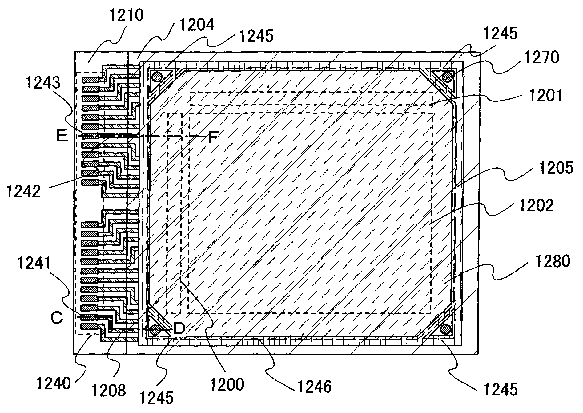
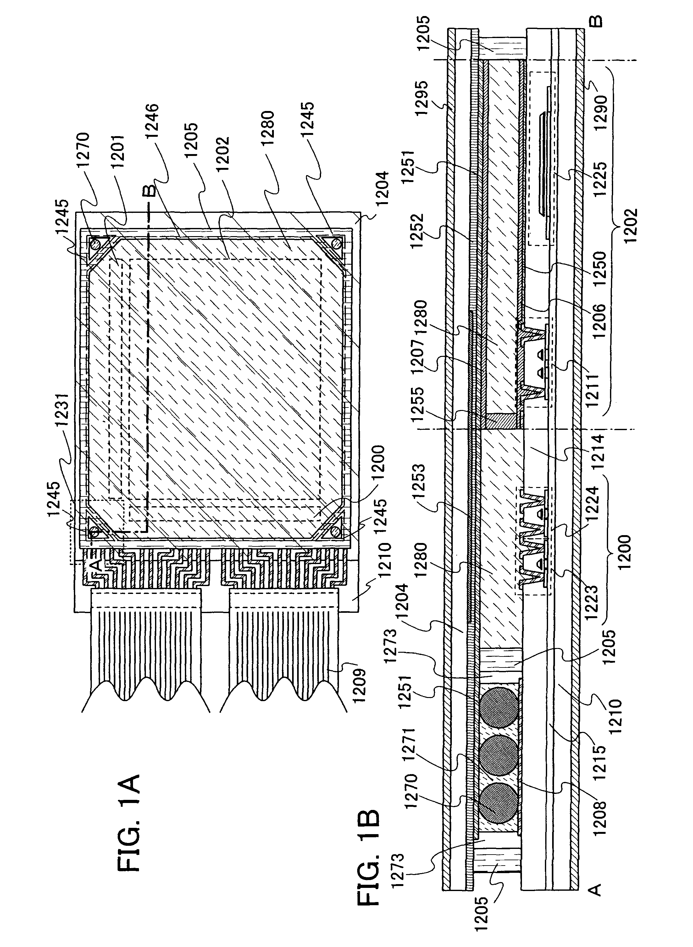
[0061]FIG. 1A is a top view of a liquid crystal display device of the present invention. A first substrate 1210 which serves as an active matrix substrate, provided with pixel electrodes and a second substrate 1204 provided with an opposite substrate are attached to each other with a first sealing material 1205, and the interior space surrounded by the first sealing material 1205 is filled with a liquid crystal 1280. A signal line driver circuit 1200, a scanning line driver circuit 1201, and a pixel region 1202 in which pixel electrodes are formed in a matrix form are formed over the first substrate 1210.

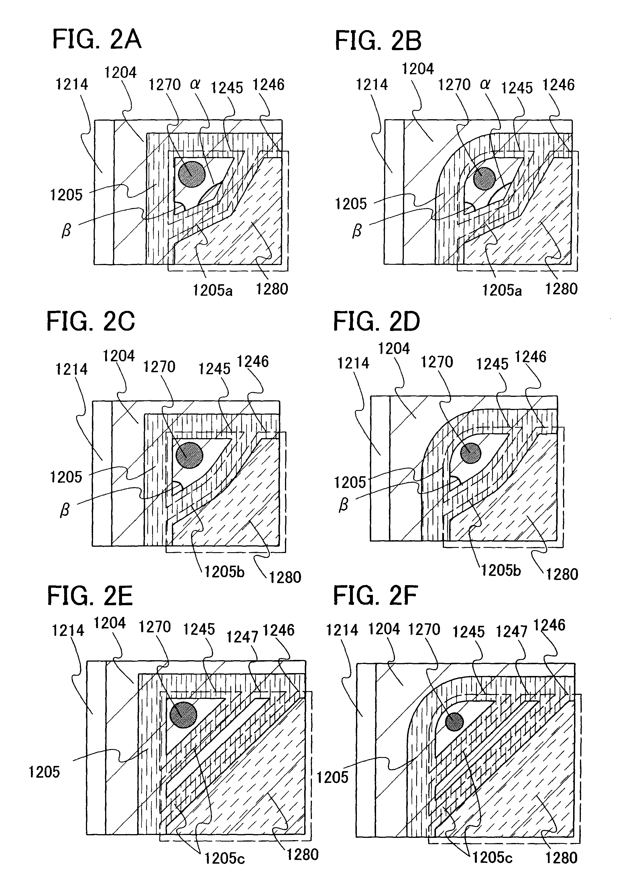
[0062]The first sealing material 1205 is also provided between the liquid crystal 1280 and a conductive particle 1270 which electrically connects a connection wiring provided for the first substrate 1210 and the opposite elect...

embodiment mode 2

[0139]According to the present invention, various electronic appliances can be formed. As examples of such an electronic appliance, the following can be given: a camera such as a video camera or a digital camera, a navigation system, a sound reproducing device (e.g., a car audio or a car audio component), a computer, a game machine, a portable information terminal (e.g., a laptop computer, a mobile phone, a portable game machine, or an electronic book), an image reproducing device provided with a storage medium (specifically, a device for reproducing the content of a storage medium such as a DVD (Digital Versatile Disc) and having a display for displaying the image), and the like.

[0140]FIG. 6A illustrates one example of a mobile phone 301. This mobile phone 301 includes a display portion 302, operating portions 303, and the like. By applying the liquid crystal display device described in Embodiment Mode 1 to the display portion 302, a display portion with less display spots and high...


PUM


Abstract

To further ensure the electrical connection of a conductor between an opposite electrode of an opposite substrate and a connection wiring of a TFT substrate, and to prevent diffusion of impurities contained in a sealing material mixed with conductive particles or a conductive paste into a liquid crystal layer. In order to isolate the sealing material containing a conductive particle or the conductive paste from the liquid crystal layer, the shape of top surface of the sealing material is a shape in which a plurality of circular shapes are combined, which is a shape having no opening. Further, the sealing material forms a plurality of compartments such that a compartment in which a pixel region is provided and a compartment in which a conductor is provided are blocked out.

Description

BACKGROUND OF THE INVENTION[0001]1. Field of the Invention[0002]The present invention relates to a method for manufacturing a liquid crystal display device. The present invention relates to, for example, a method for manufacturing an electro-optical device typified by a liquid crystal display panel which has a circuit including a thin film transistor (hereinafter referred to as a TFT), and a method for manufacturing an electronic device equipped with such an electro-optical device as a component.[0003]2. Description of the Related Art[0004]In recent years, a technique for forming a thin film transistor (TFT) using a semiconductor thin film (with a thickness of about several nm to several hundreds nm) which is formed over a substrate having an insulating surface has attracted attention. The thin film transistor is widely applied to an electronic device such as an IC or an electro-optical device, and has been hurriedly developed particularly as a switching element of an image display ...

Claims


Application Information

Patent Timeline
IPC IPC(8): G02F1/1339
CPCG02F1/1339G02F1/1345G02F2001/13415G02F1/13415
Inventor ISHITANI, TETSUJI
Owner SEMICON ENERGY LAB CO LTD
Why Eureka
Try Eureka