Eureka AIR delivers breakthrough ideas for toughest innovation challenges, trusted by R&D personnel around the world.

Liquid material discharge method, wiring substrate manufacturing method, color filter manufacturing method, and organic el element manufacturing method

a technology of organic el element and discharge method, which is applied in the manufacture of printed circuits, coatings, electroluminescent light sources, etc., can solve the problems of inability to disclose the manner, remains a risk of flying deflection, and cannot be eliminated, so as to achieve high precision, high precision, and satisfying precision

Inactive Publication Date: 2008-11-20
SEIKO EPSON CORP
View PDF4 Cites 10 Cited by
  • Summary
  • Abstract
  • Description
  • Claims
  • Application Information

AI Technical Summary

Benefits of technology

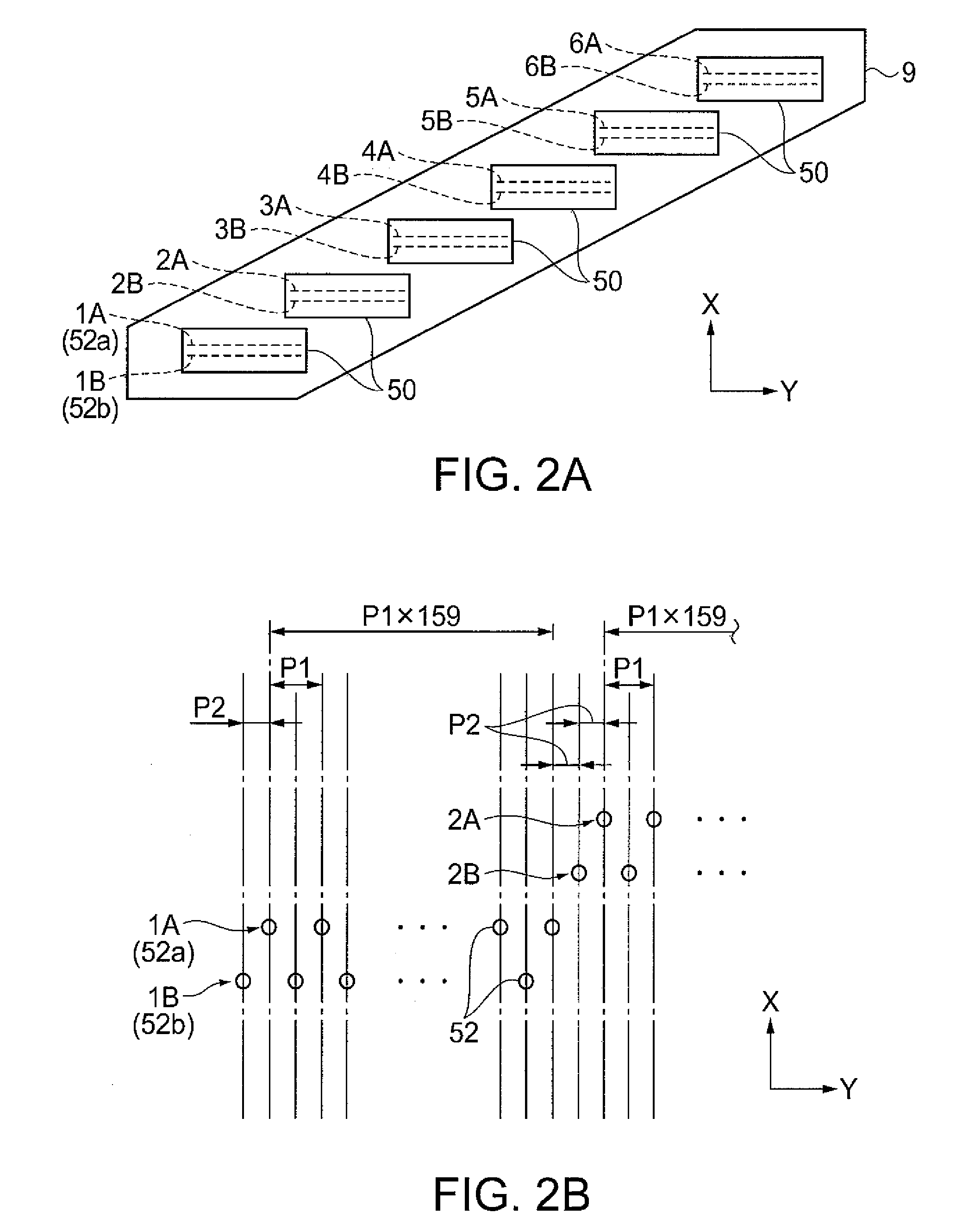
The present invention provides a liquid material discharge method that can control the driving of a discharge head to cause droplets to land with satisfactory precision. The method includes steps for positioning the substrate and discharge head, and discharging droplets onto the substrate in synchronization with primary scanning. The method can vary the discharge timing for a prescribed nozzle and drive the discharge head based on landing position information of the droplets to land them with precision. The method can also correct flying deflection in the primary scanning direction by generating a second arrangement pattern and driving the discharge head based on the landing position information for the first arrangement pattern. The method can acquire the landing position information and use it to generate the second arrangement pattern. Overall, the liquid material discharge method provides precise control over droplet discharge and is useful in various manufacturing processes.

Problems solved by technology

However, there is no clear disclosure of the manner in which the control signal for driving the droplet discharge head is generated based on the detected landing position and landed diameter.
Particularly when the landing position deviates due to flying deflection, the direction in which the landing position deviates due to flying deflection is not necessarily fixed, and the solution to this problem is unclear.
However, the causes of flying deflection cannot be eliminated even by such restoration operations, and there remains a risk of flying deflection.

Method used


Image

  • Liquid material discharge method, wiring substrate manufacturing method, color filter manufacturing method, and organic el element manufacturing method
  • Liquid material discharge method, wiring substrate manufacturing method, color filter manufacturing method, and organic el element manufacturing method
  • Liquid material discharge method, wiring substrate manufacturing method, color filter manufacturing method, and organic el element manufacturing method

Examples


first embodiment

Liquid Material Discharge Method and Wiring Substrate Manufacturing Method

[0079]The liquid material discharge method of the present invention will next be described using the example of the wiring board manufacturing method in which the liquid material discharge method is applied.

[0080]FIG. 6 is a schematic plan view showing the wiring substrate. As shown in FIG. 6, the wiring substrate 300 is a circuit substrate for planar packaging of a semiconductor device (IC), and is composed of an insulation film 307, and input wiring 301 and output wiring 303 composed of a conductive material that is arranged to correspond to input and output electrodes (bumps) of the IC. The insulation film 307 is formed clear of the input terminal parts 302 and the output terminal parts 304, and covers the plurality of input wiring 301 and output wiring 303 so that the input wiring 301 and the output wiring 303 are each partially exposed in the packaging region 305. The wiring substrates 300 are formed in a...

second embodiment

[0107]Referring now to FIGS. 10 to 12, a color filter manufacturing method in accordance with a second embodiment will now be explained. In view of the similarity between the first and second embodiments, the parts of the second embodiment that are identical to the parts of the first embodiment will be given the same reference numerals as the parts of the first embodiment. Moreover, the descriptions of the parts of the second embodiment that are identical to the parts of the first embodiment may be omitted for the sake of brevity.

[0108]The color filter manufacturing method will next be described as another embodiment in which the liquid material discharge method of the first embodiment is applied.

[0109]The liquid crystal display device as an electro-optical device having a color filter will first be briefly described. FIG. 10 is a schematic perspective view showing the structure of the liquid crystal display device. As shown in FIG. 10, the liquid crystal display device 500 of the p...

third embodiment

[0132]Referring now to FIGS. 13 and 14, an organic EL element manufacturing method in accordance with a third embodiment will now be explained. In view of the similarity between the first and third embodiments, the parts of the third embodiment that are identical to the parts of the first embodiment will be given the same reference numerals as the parts of the first embodiment. Moreover, the descriptions of the parts of the third embodiment that are identical to the parts of the first embodiment may be omitted for the sake of brevity.

[0133]The organic EL element manufacturing method will next be described as another embodiment in which the liquid material discharge method of the first embodiment is applied.

[0134]The organic EL display device having the organic EL element will first be briefly described.

[0135]FIG. 13 is a schematic sectional view showing the relevant parts of the structure of the organic EL display device. As shown in FIG. 13, the organic EL display device 600 is pro...


PUM

PropertyMeasurementUnit
movementaaaaaaaaaa
nozzle diameteraaaaaaaaaa

Abstract

A liquid material discharge method includes positioning a substrate and a discharge head having a plurality of nozzles to face each other, discharging droplets of a liquid material including a functional material onto the substrate in synchronization with a primary scanning for moving the discharge head and the substrate in relative manner, and varying one of a discharge timing and a discharge rate for discharging the droplets from at least one of the nozzles based on landing position information of the droplets that are discharged from the nozzles.

Description

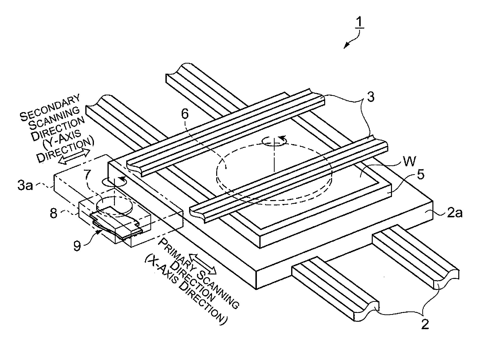
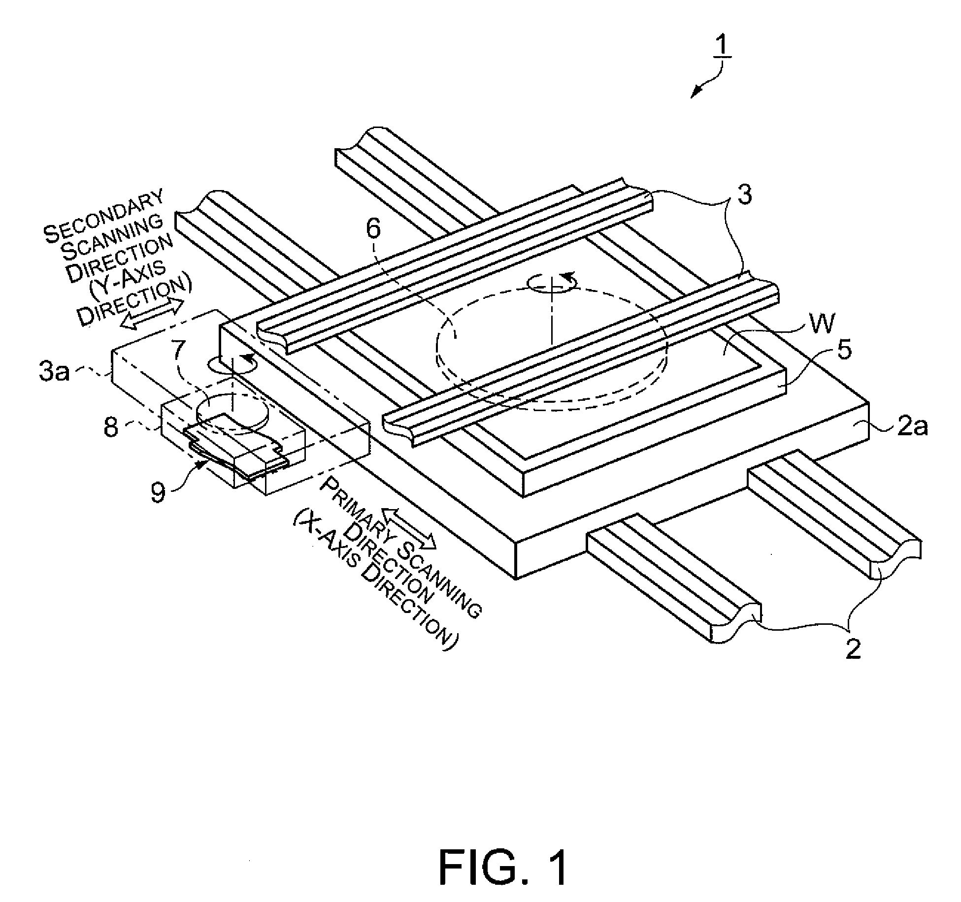
CROSS-REFERENCE TO RELATED APPLICATIONS[0001]This application claims priority to Japanese Patent Application No. 2006-220016 filed on Aug. 11, 2006. The entire disclosure of Japanese Patent Application No. 2006-220016 is hereby incorporated herein by reference.BACKGROUND OF THE INVENTION[0002]1. Technical Field[0003]The present invention relates to a method for discharging a liquid material that includes a functional material, to a method for manufacturing a wiring substrate, to a method for manufacturing a color filter, and to a method for manufacturing an organic EL luminescent element.[0004]2. Related Art[0005]Japanese Laid-Open Patent Application Publication No. 2006-15243 discloses a method for discharging a liquid material that includes a functional material include a method for forming a desired film pattern on a substrate. This method for forming a film pattern comprises a detection step for discharging droplets of a functional material from a droplet discharge head prior to...

Claims


Application Information

Patent Timeline
Patent Type & Authority Applications(United States)
IPC IPC(8): B05D1/02
CPCH01L51/0005H01L51/56H05B33/10H05K3/125H05K2203/013H10K71/135H10K71/40H10K71/00
Inventor USHIYAMA, YOSHIHIKOKITAHARA, TSUYOSHIMIYASAKA, YOICHI
Owner SEIKO EPSON CORP
Why Eureka
Eureka Blog
Learn More