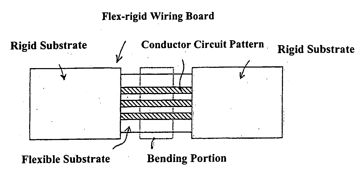
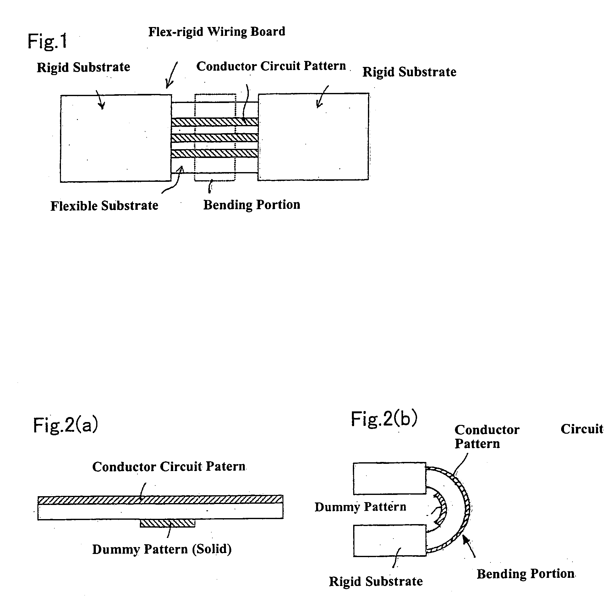
Flex-Rigid Wiring Board and Manufacturing Method Thereof
a technology of flexible wiring board and manufacturing method, which is applied in the direction of resistive material coating, metallic material coating process, electrical equipment, etc., can solve the problems of insufficient strength, inability to show good results in thermo cycle test or similar reliability test, and inability to ensure high connection reliability, etc., to achieve easy bending of flexible substrate, increase rigidity, and less dimension variation
- Summary
- Abstract
- Description
- Claims
- Application Information
AI Technical Summary
Benefits of technology
Problems solved by technology
Method used
Image

Examples
example 1
(A) Preparation of a Flexible Substrate
[0242](1) As a starting material for a flexible substrate 100A as a member to manufacture a flex-rigid printed wiring board according to an embodiment of the present invention, there was used a 50 μm-thick double-sided copper-clad laminate (E-67 by HITACHI CHEMICAL) in which an 18 μm-thick copper foil 12 was laminated on either side of an insulative base material 11 formed by impregnating a 20 μm-thick glass cloth (whose thickness may be less than 30 μm and whose glass fibers had a mean thickness of 4.0 μm) with epoxy resin and drying it. See FIG. 11(a).
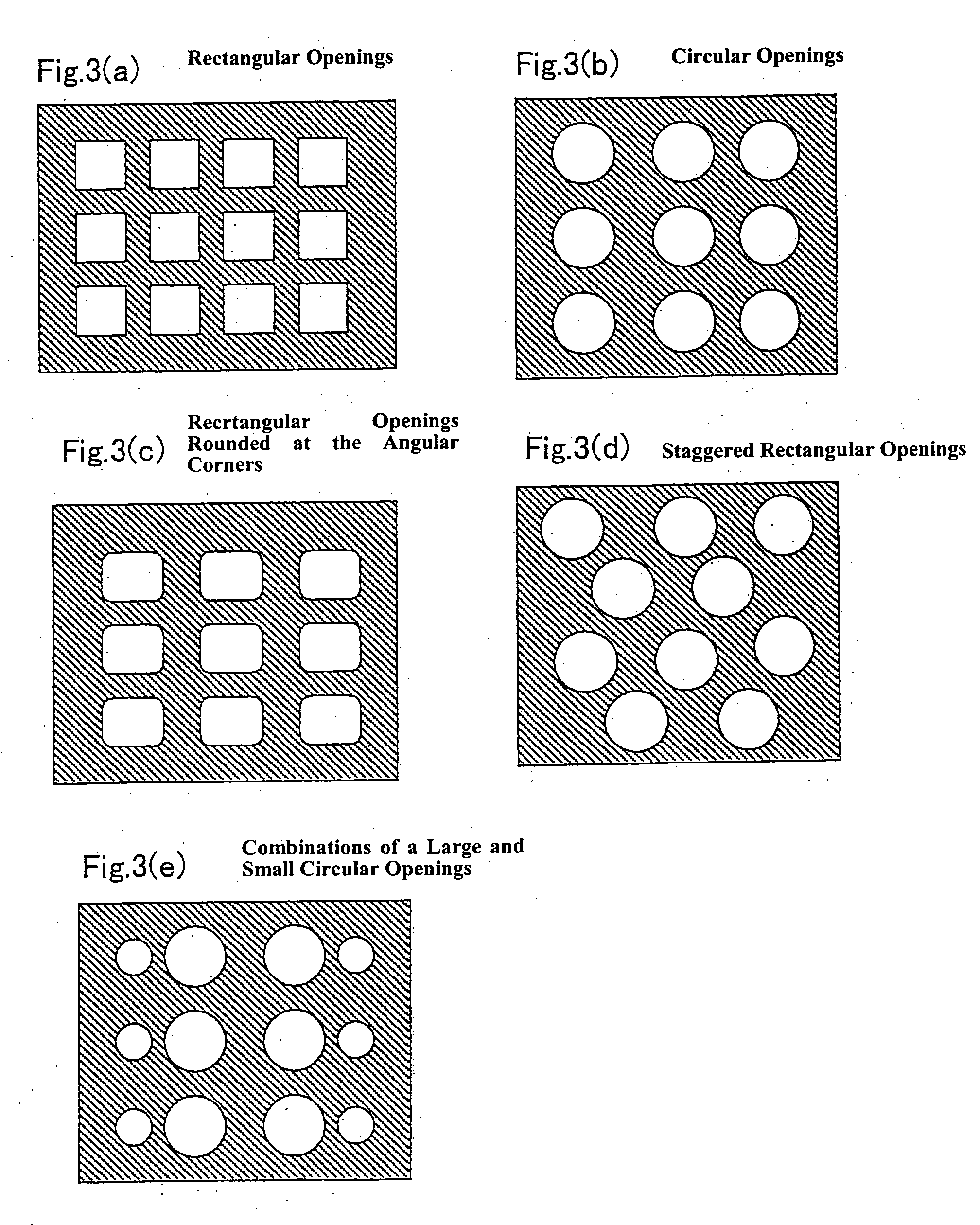
[0243](2) The copper foil 12 laminated on either side of the insulative film 11 was etched with a cupric chloride aqueous-solution to form a conductor circuit pattern 13 whose line width was 300 μm and 250 μm-diameter interconnecting electrode pads 16 on one side of the insulative base material. A lattice-shaped dummy pattern 18 (having formed therein openings each having a rectangular shape and...
example 2
[0255]There was manufactured a flex-rigid printed wiring board 300A similar to the example 1 except that there was formed around the bending portion of the flexible substrate a lattice-shaped dummy pattern 18 having formed therein openings each having a rectangular shape and an area of 40,000 μm2, the ratio between the sum of the areas of all the openings and the area of the rest of the lattice pattern being 9:10.
example 3
[0256]There was manufactured a flex-rigid printed wiring board 300A similar to the example 1 except that there was formed around the bending portion of the flexible substrate a lattice-shaped dummy pattern 18 having formed therein openings each having a rectangular shape and an area of 90,000 μm2, the ratio between the sum of the areas of all the openings and the area of the rest of the lattice pattern being 11:10.
PUM
| Property | Measurement | Unit |
|---|---|---|
| Thickness | aaaaa | aaaaa |
| Thickness | aaaaa | aaaaa |
| Thickness | aaaaa | aaaaa |
Abstract
Description
Claims
Application Information
 - Generate Ideas
- Intellectual Property
- Life Sciences
- Materials
- Tech Scout
- Unparalleled Data Quality
- Higher Quality Content
- 60% Fewer Hallucinations
Browse by: Latest US Patents, China's latest patents, Technical Efficacy Thesaurus, Application Domain, Technology Topic, Popular Technical Reports.
© 2025 PatSnap. All rights reserved.Legal|Privacy policy|Modern Slavery Act Transparency Statement|Sitemap|About US| Contact US: help@patsnap.com