Memory cell and method for manufacturing the same

a memory cell and manufacturing method technology, applied in the field of memory cells, can solve the problems of insufficient drive current to perform operations, insufficient capacitance area between the floating gate and the control gate, and high cost of memory cells to manufacture, so as to improve the electrical performance of the memory cell during operation, suppress current leakage at the top corners of the fin structure, and increase the level of integration

Active Publication Date: 2008-11-27
MACRONIX INT CO LTD
View PDF15 Cites 22 Cited by
  • Summary
  • Abstract
  • Description
  • Claims
  • Application Information

AI Technical Summary

Benefits of technology

[0008]The present invention provides a memory cell possessing a doped region / doped cap layer disposed on the fin structure which overcomes the current leakage problem during the operations of the memory cell.
[0009]The present invention provides a method for manufacturing memory cells capable of decreasing the step height of each memory cell having fin structure and increasing the integration of the memory cells.
[0034]In the present invention, by performing a surface treatment to form either a doped region in the fin structure or a doped polysilicon cap layer on the fin structure with the conductive type complementary to that of the channel between the source / drain regions, the current leakage at the top corners of the fin structure can be suppressed and the electrical performance of the memory cell during operation is improved. The present invention also makes use of trimming process to miniaturize the patterned mask layer and to form memory cells having fin-structures in the substrate. The present invention increases the level of integration using simple and inexpensive methods.

Problems solved by technology

Nevertheless, as memory cells shrink, the capacitance area between the floating gate and the control gate has to shrink as well.
As a result, the size of the drive current is usually insufficient to perform operations such as programming, erasing and reading.
However, these types of memory cells are expensive to manufacture and the fabrication process are complex.
Further, the throughput of such memory cells is low.
Moreover, in tri-gate memory cells, current leakage occurs at the corners of such device, and current leakage is worsened when the device is operated under high electric field.
As a result, the reliability and stability of the memory device lowers and decreasing the production yield.

Method used


Image

  • Memory cell and method for manufacturing the same
  • Memory cell and method for manufacturing the same
  • Memory cell and method for manufacturing the same

Examples


Embodiment Construction

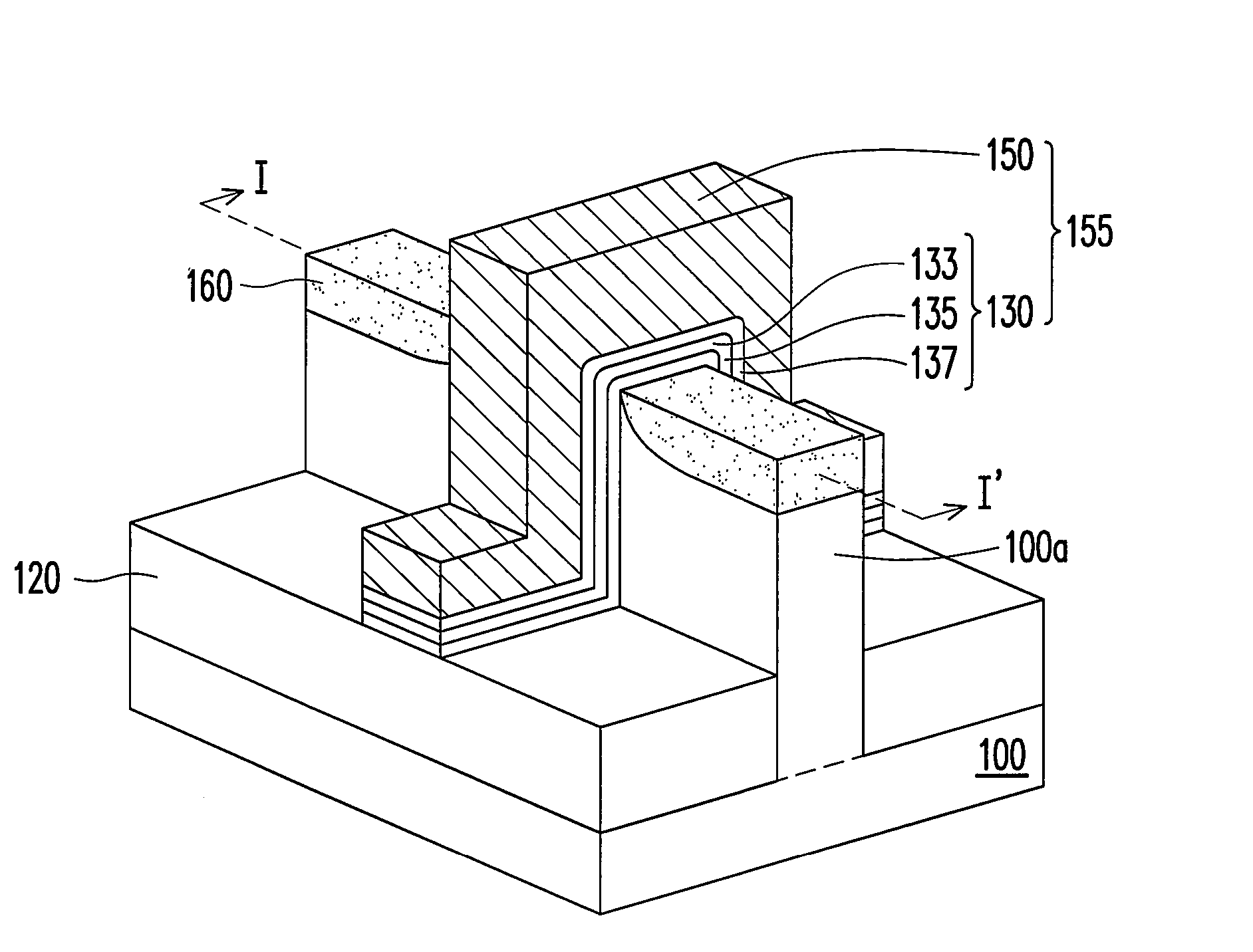
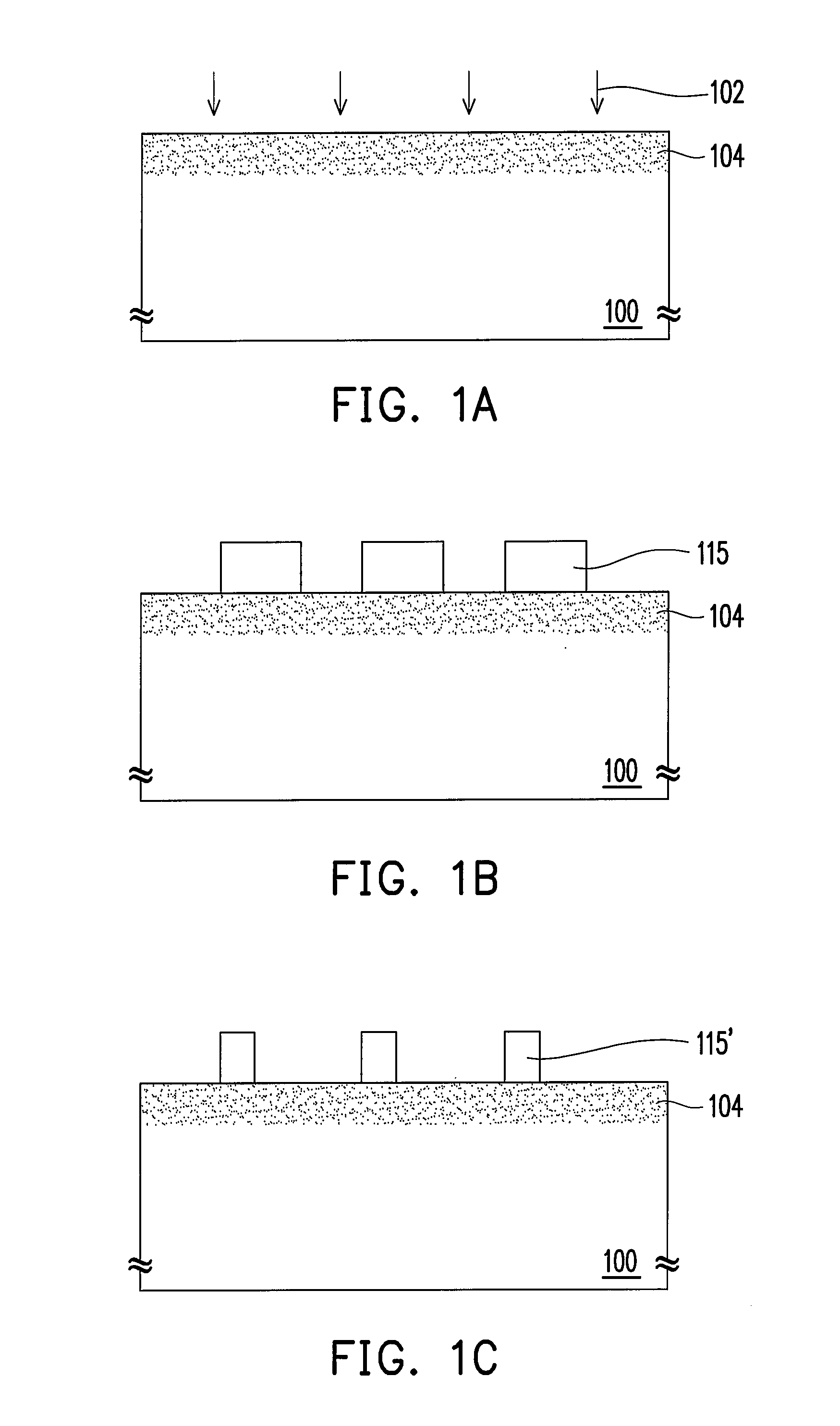
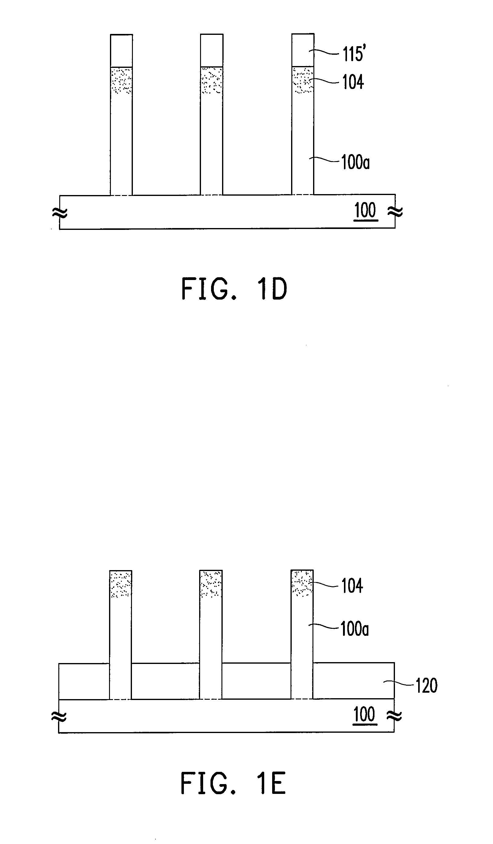
[0042]FIGS. 1A through 1G are schematic cross-sectional views illustrating the steps for manufacturing a memory cell according to one embodiment of the present invention.

[0043]As shown in FIG. 1A, the present invention provides a method for manufacturing memory cells. First, a substrate 100 is provided. The substrate can be a bulk-Si substrate or a silicon-on-insulator (SOI) substrate. A surface treatment 102 is performed on the substrate 100 so as to form a doped region 104 in the substrate 100 and near the surface of the substrate 100. It should be noticed that the conductive type of the doped region 104 is complementary to the conductive type of the later formed channel region of the memory cell in order to suppress the current leakage due to the corner edge effect during the operation of memory cells. That is, when the memory cell has an n-type channel region, the doped region 104 is a p-type doped region, and vice versa. The thickness of the doped region 104 in the substrate 10...


PUM


Abstract

The invention provides a memory cell. The memory cell is disposed on a substrate and comprises a plurality of isolation structures defining at least a fin structure in the substrate. Further, the surface of the fin structure is higher than the surface of the isolation structure. The memory cell comprises a doped region, a gate, a charge trapping structure and a source / drain region. The doped region is located in a top of the fin structure and near a surface of the top of the fin structure and the doped region has a first conductive type. The gate is disposed on the substrate and straddled the fin structure. The charge trapping structure is disposed between the gate and the fin structure. The source / drain region with a second conductive type is disposed in the fin structures exposed by the gate and the first conductive type is different from the second conductive type.

Description

CROSS-REFERENCE TO RELATED APPLICATION[0001]This application claims the priority benefit of U.S. provisional application Ser. No. 60 / 980,792, filed on Oct. 18, 2007, and is a continuation-in-part of a prior application Ser. No. 11 / 753,850, filed May 25, 2007. The entirety of each of the above-mentioned patent applications is incorporated herein by reference and made a part of this specification.BACKGROUND OF THE INVENTION[0002]1. Field of the Invention[0003]The present invention relates to a semiconductor device, the manufacturing method and the operating method thereof. More particularly, the present invention relates to a memory cell, the manufacturing method and the operating method thereof.[0004]2. Description of Related Art[0005]Along with the development of integrated circuits technology, the level of integration has to increase continuously in order to improve the device speed and functions. Take memory structure for example. When information electronic products (such as comp...

Claims


Application Information

Patent Timeline
Patent Type & Authority Applications(United States)
IPC IPC(8): H01L21/8247H01L27/115G11C11/34
CPCH01L21/28282H01L21/84H01L27/115H01L27/11568H01L27/12H01L29/66833H01L29/792H01L29/40117H10B43/30H10B69/00
Inventor HSU, TZU-HSUANLUE, HANG-TING
Owner MACRONIX INT CO LTD
Why Eureka
Try Eureka