SiGe or SiC layer on STI sidewalls

a sige or sic layer technology, applied in the direction of semiconductors, electrical devices, transistors, etc., can solve the problems of increasing the relaxation effect of the stress applied by the sige or sic stressor, the conventional methods of improving the performance of the metal-oxide-semiconductor, and the mos has run into bottlenecks, so as to reduce the stress relaxation effect and improve the stress applied

Inactive Publication Date: 2008-11-27
TAIWAN SEMICON MFG CO LTD
View PDF12 Cites 20 Cited by
  • Summary
  • Abstract
  • Description
  • Claims
  • Application Information

AI Technical Summary

Benefits of technology

[0010]The advantageous features of the present invention include improvements in stress applied to channel regions of MOS device, and the reduction in the stress relaxation effect.

Problems solved by technology

With the continuous scaling of integrated circuits, the conventional methods for improving performance of metal-oxide-semiconductor (MOS) devices, such as shortening gate lengths of MOS devices, has run into bottlenecks.
Although conventional MOS devices with SiGe stressors or SiC stressors exhibited excellent performance, with the down-scaling of integrated circuits, particularly to 32 nm technology or below, the relaxation effect that occurs on the stresses applied by the SiGe or SiC stressors become increasingly more severe.
Hence, the stresses in the resulting MOS devices cannot meet design requirements.

Method used


Image

  • SiGe or SiC layer on STI sidewalls
  • SiGe or SiC layer on STI sidewalls
  • SiGe or SiC layer on STI sidewalls

Examples


Embodiment Construction

[0014]The making and using of the presently preferred embodiments are discussed in detail below. It should be appreciated, however, that the present invention provides many applicable inventive concepts that can be embodied in a wide variety of specific contexts. The specific embodiments discussed are merely illustrative of specific ways to make and use the invention, and do not limit the scope of the invention.

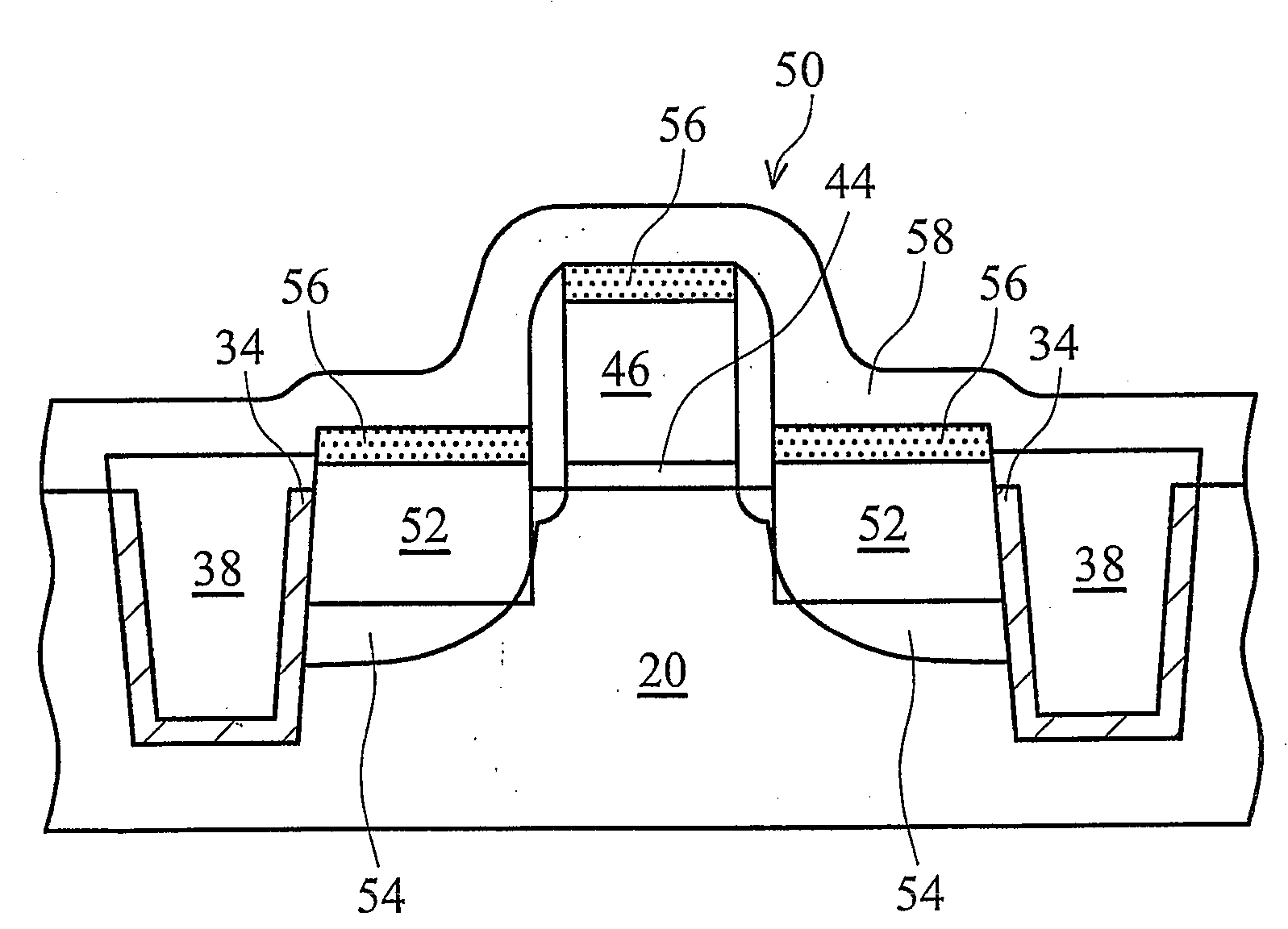
[0015]A novel shallow trench isolation (STI) structure for providing a stress to channel regions of metal-oxide-semiconductor (MOS) devices and methods of forming the same are provided. The intermediate stages in the manufacturing a preferred embodiment of the present invention are illustrated. The variations of the preferred embodiment are then discussed. Throughout the various views and illustrative embodiments of the present invention, like reference numbers are used to designate like elements.

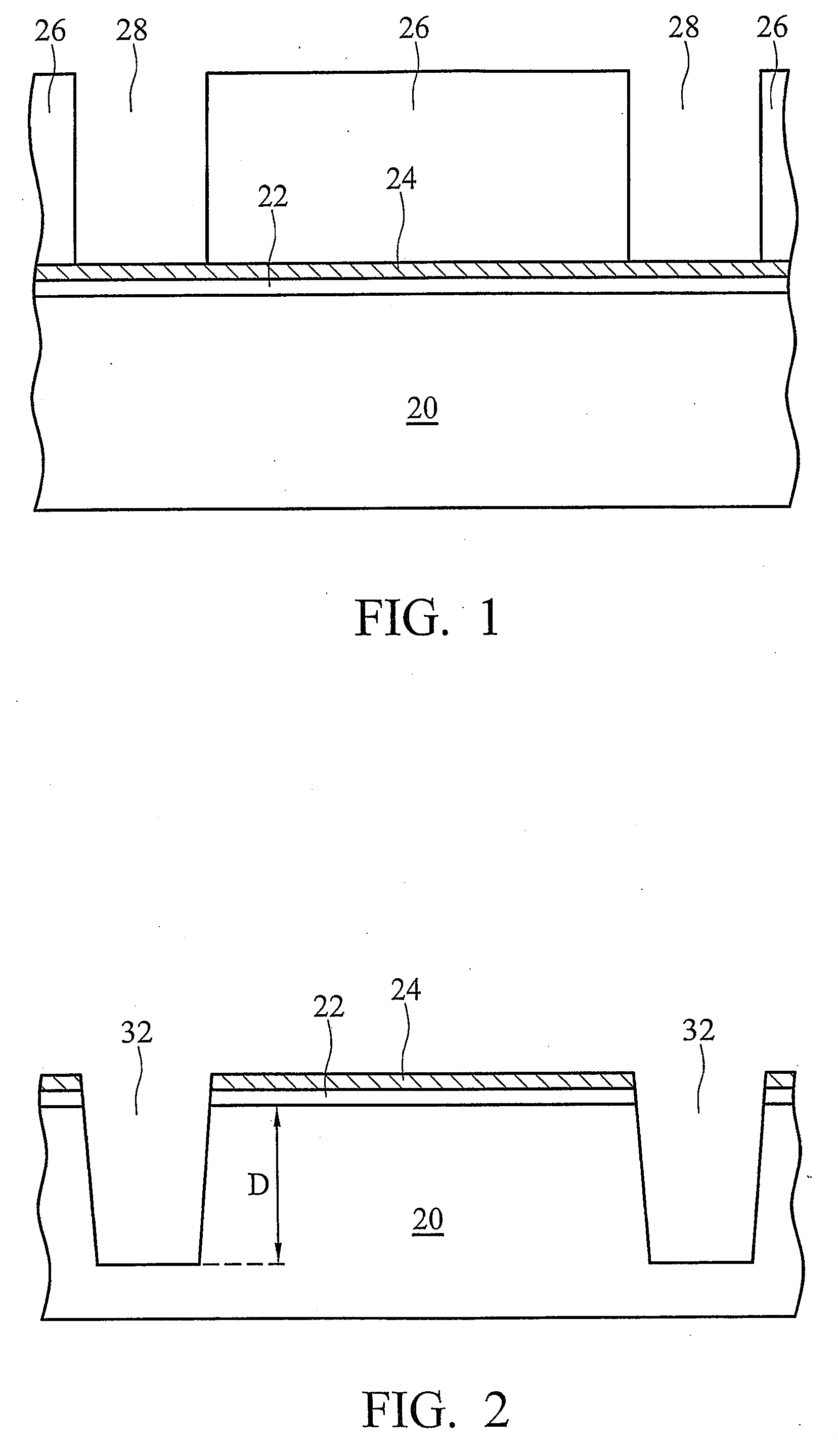
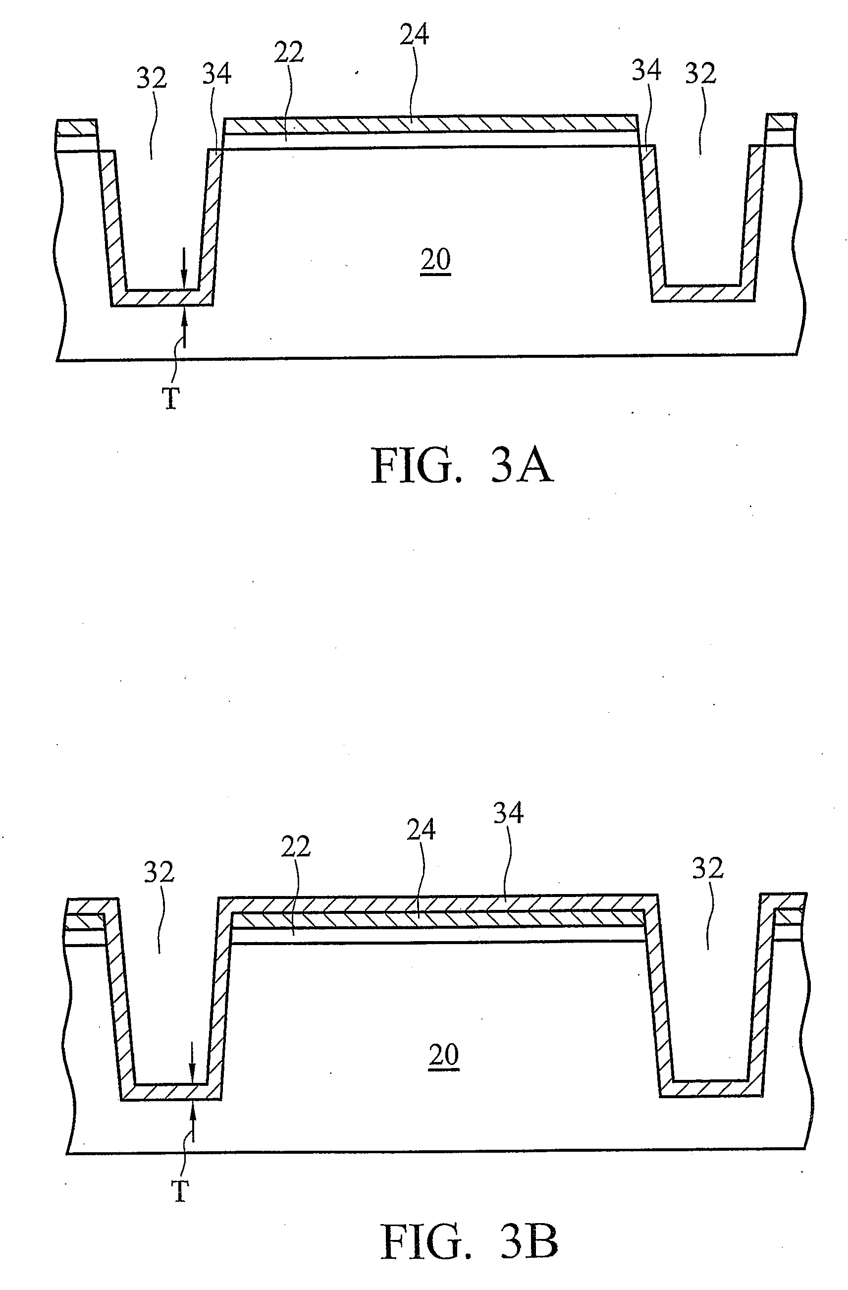
[0016]Referring to FIG. 1, semiconductor substrate 20 is provided. In the prefer...


PUM


Abstract

A semiconductor structure includes a semiconductor substrate; an opening in the semiconductor substrate; a semiconductor layer in the opening and covering a bottom and sidewalls of the opening, wherein the semiconductor layer and the semiconductor substrate comprise different materials; and a dielectric material over the semiconductor layer and filling a remaining portion of the opening.

Description

TECHNICAL FIELD[0001]This invention relates generally to integrated circuits, and more particularly to structures and manufacturing methods of shallow trench isolation regions.BACKGROUND[0002]Reductions in sizes and inherent features of semiconductor devices have enabled continued improvements in speed, performance, density, and cost per unit function of integrated circuits over the past few decades. With the continuous scaling of integrated circuits, the conventional methods for improving performance of metal-oxide-semiconductor (MOS) devices, such as shortening gate lengths of MOS devices, has run into bottlenecks. To further enhance the performance of MOS devices, stress may be introduced in the channels of the MOS devices to improve carrier mobility. Generally, it is desirable to induce a tensile stress in the channel region of an n-type MOS (NMOS) device in a source-to-drain direction and to induce a compressive stress in the channel region of a p-type MOS (PMOS) device in a so...

Claims


Application Information

Patent Timeline
Patent Type & Authority Applications(United States)
IPC IPC(8): H01L27/092H01L21/336H01L29/78
CPCH01L21/823807H01L21/823878H01L29/665H01L29/6659H01L29/7833H01L29/7846
Inventor YU, MING-HUAHUANG, TAI-CHUNCHEN, CHIEN-HAOKU, KEH-CHIANGLI, JR.-HUNGYEH, LING-YENLEE, TZE-LIANG
Owner TAIWAN SEMICON MFG CO LTD
Why Eureka
Try Eureka