Modification of pb-free solder alloy compositions to improve interlayer dielectric delamination in silicon devices and electromigration resistance in solder joints

a technology of pb-free solder alloys and alloy compositions, which is applied in the direction of manufacturing tools, soldering apparatus, transportation and packaging, etc., can solve the problems of interfacial voids and compromise the structural integrity of solder joints, and achieve good mechanical integrity and reliability

Inactive Publication Date: 2009-08-06
SHIH YUAN +5
View PDF6 Cites 61 Cited by
  • Summary
  • Abstract
  • Description
  • Claims
  • Application Information

AI Technical Summary

Benefits of technology

[0010]It is an object of the invention to provide a solder joint having good mechanical integrity and reliability as a function of thermal aging time at elevated temperatures, such as those that may be realized under field operational conditions.

Problems solved by technology

The formation of interfacial voids is undesirable in that it compromises the structural integrity of solder joints when the void densities become high.

Method used


Image

  • Modification of pb-free solder alloy compositions to improve interlayer dielectric delamination in silicon devices and electromigration resistance in solder joints
  • Modification of pb-free solder alloy compositions to improve interlayer dielectric delamination in silicon devices and electromigration resistance in solder joints
  • Modification of pb-free solder alloy compositions to improve interlayer dielectric delamination in silicon devices and electromigration resistance in solder joints

Examples


example 1

[0052]A 0.025 inch (0.635 mm) diameter solder ball is reflowed on a single 0.022 inch (0.559 mm) diameter Cu pad, voiding is prevented, with only 0.1 wt % Zn in the initial solder ball.

example 2

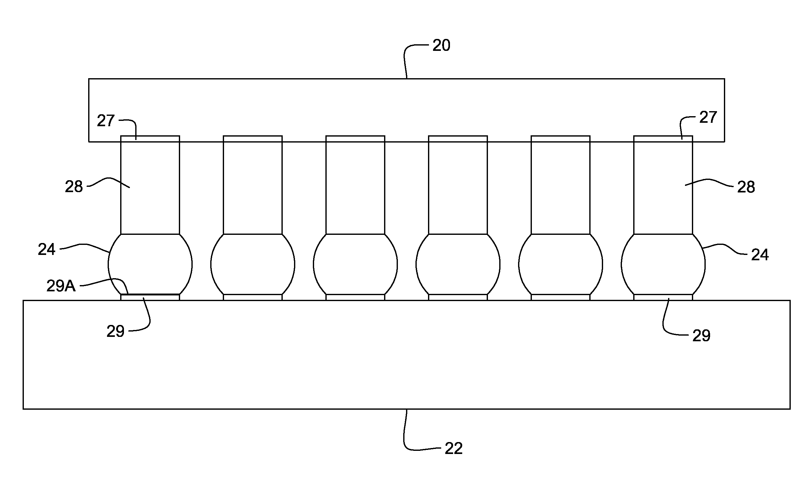
[0053]A solder joint is created with two opposed Cu pads, using a 0.025 inch (0.635 mm) diameter solder ball and 0.022 inch (0.559 mm) diameter pads, some voiding is found with 0.1 wt % Zn present in the initial solder ball. The outcome with one Cu pad and one Ni pad remains undefined for these ball and pad sizes. But, Zn does react at the Ni pad surface. With 0.3 wt % Zn in the solder and the same ball and pad geometry, voiding is prevented with dual Cu pads. Thus, for these typical BGA situations, generally 0.6 or less % wt Zn is more than adequate to suppress void growth.

[0054]The important metric in this situation is the ratio of the quantity of available Zn in the solder to the pad surface area. This relationship may be expressed in units of grams of Zn per square micron (μ2) of pad area. In the case and associated geometry described above, based on the fact that 0.1 wt % Zn is barely adequate for the ball and pad geometry, with a single Cu pad (but not two pads), and ignoring ...

example 3

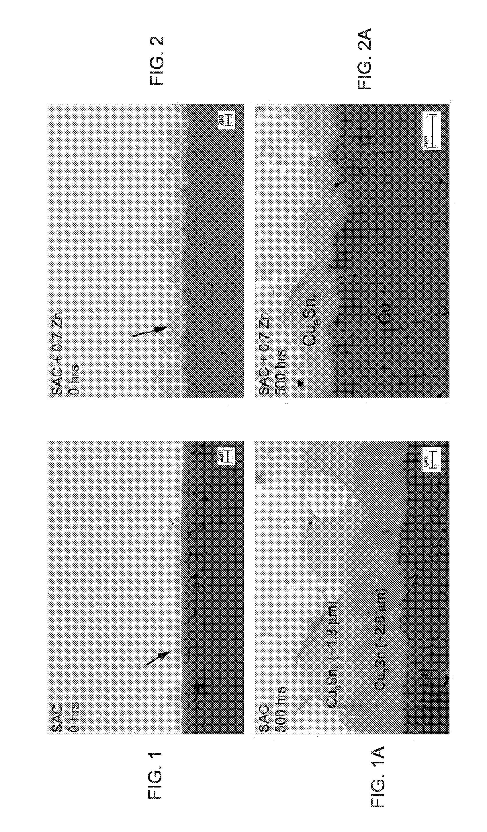
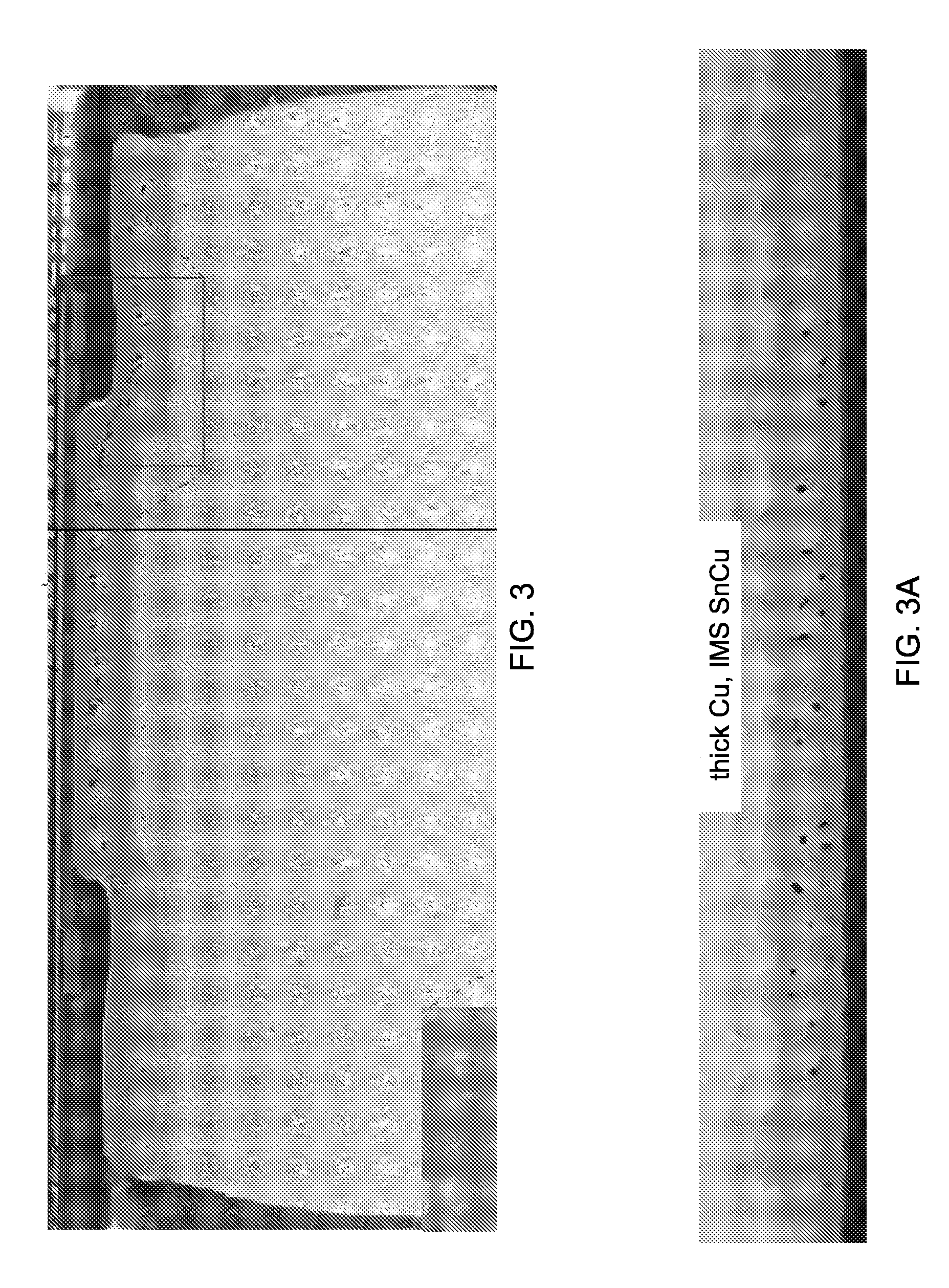
[0062]In the case of high-Sn lead containing solders (such as Sn-37Pb) on Cu-based pad structures, excessive pore formation is far from typical. However, in 5-10% of all Cu pad structures, testing leads to severe voiding in the Cu3Sn layer. Moreover, extrapolation of accelerated aging results by means of an empirical Arrhenius dependence may be seen to overestimate “life in service” by a factor of 40 or more, under some circumstances. This situation derives from the fact that the growth rate of the voids can be highly variable and the degree of voiding is seen to depend completely on the nature of the Cu pad and has its origins in the plating process used to create the pad structure. Generally, excessive void formation has not been found when high purity, wrought Cu is used. However, under certain conditions it occurs sporadically with plated Cu structures currently supplied to the electronics industry and leads to solder joint fragility. However, voiding may also be significantly r...


PUM

PropertyMeasurementUnit
temperatureaaaaaaaaaa
melting pointaaaaaaaaaa

Abstract

A solder joint comprising a solder capture pad on a substrate having a circuit; and a lead free solder selected from the group comprising Sn—Ag—Cu solder and Sn—Ag solder adhered to the solder capture pad; the solder selected from the group comprising between 0.1 to 2.0% by weight Sb or Bi, and 0.5 to 3.0% Ag. Formation of voids at an interface between the solder and the solder capture pad is suppressed, by including Zn. Interlayer dielectric delamination is suppressed, and electromigration characteristics are greatly improved. Methods for forming solder joints using the solders.

Description

[0001]This application is a continuation-in-part of U.S. patent application Ser. No. 12 / 181,305 filed on Jul. 28, 2008, which is a continuation-in-part of Ser. No. 11 / 669,076 filed on Jan. 30, 2007.BACKGROUND OF THE INVENTION[0002]1. Field of the Invention[0003]The present invention relates applications for predominantly lead free solders and methods of forming solder joints and related interconnect structures using such solders. While it is related to solders generally, more particularly, the invention relates to the addition of minor alloying additives such as zinc, bismuth, or antimony for suppressing interlayer dielectric delamination and electromigration in Sn based lead-free solders comprising tin and copper, and solder comprising tin, silver and copper.[0004]2. Background Art[0005]There has been an extensive search for Pb-free, solder, alloys in recent years. Several promising candidates have been identified for different soldering applications, which include Sn-0.7Cu, Sn-3.5...

Claims


Application Information

Patent Timeline
Patent Type & Authority Applications(United States)
IPC IPC(8): B32B15/01B23K1/20
CPCB23K1/0016B23K1/008B23K1/203Y10T428/12708C22C13/00H05K3/3463Y10T428/12715B23K2201/42B23K2101/42H01L2224/16225
Inventor SHIH, DA-YUANHENDERSON, DONALD W.KANG, SUNG K.LU, MINHUANAH, JAE-WOONGSRIVASTAVA, KAMALESH
Owner SHIH YUAN
Why Eureka
Try Eureka