White Multi-Wavelength LED and Its Manufacturing Process

a technology of light-emitting diodes and manufacturing processes, which is applied in the direction of electric lighting sources, semiconductor devices, and light-emitting sources. it can solve the problems of compromising the luminance and color performance of the entire led, and achieve the effect of promoting the luminance performance of the led

Inactive Publication Date: 2008-11-27
LEE MING SHUN
View PDF4 Cites 3 Cited by
  • Summary
  • Abstract
  • Description
  • Claims
  • Application Information

AI Technical Summary

Benefits of technology

[0007]The primary purpose of the present invention is to provide a white multi-wavelength LED to produce the expected white light and effectively promote luminance performance. To achieve the purpose, a die unit for a white multi-wavelength LED is comprised of having at the bottom of a light emitting chip in a given color bonded with a first non-conductive material containing phosphor in a color corresponding to that of the chip. The first non-conductive material functions as the position to coat the encapsulating material to secure the die unit to the carrier. Golden plated wire is used as circuit connection for the light emitting chip, and finally, a second non-conductive material containing phosphor in a color corresponding to that of the chip is injected to cover up the light emitting chip to allow the light from the chip to pass through both of the first and the second non-conductive materials and to be incorporated with the wavelength of the phosphor respectively contained in both of the first and the second non-conductive materials.
[0009]A reflection material may be further disposed at the bottom of the first non-conductive material to help promote the luminance performance of the LED.

Problems solved by technology

However, the construction of a white LED illustrated in FIG. 1 of having an encapsulating material 40 directly embedded at the bottom of a blue light emitting chip 21, the light travel or the extent of the phosphor is excited may vary depending on the level of the encapsulating material 40 is embedded, thus to compromise the luminance and color performance of the entire LED.

Method used


Image

  • White Multi-Wavelength LED and Its Manufacturing Process
  • White Multi-Wavelength LED and Its Manufacturing Process
  • White Multi-Wavelength LED and Its Manufacturing Process

Examples


Embodiment Construction

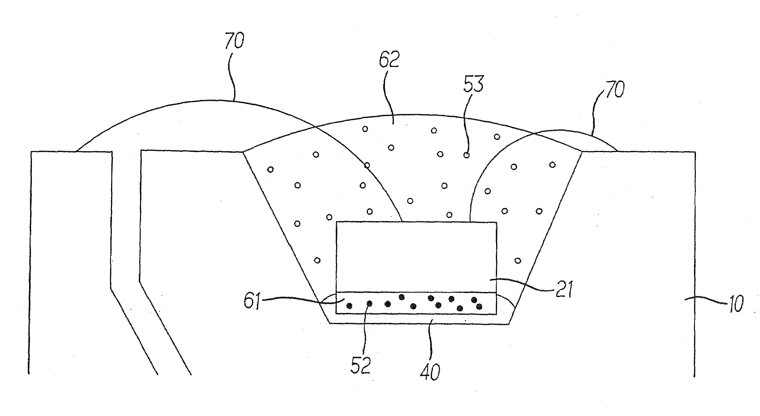
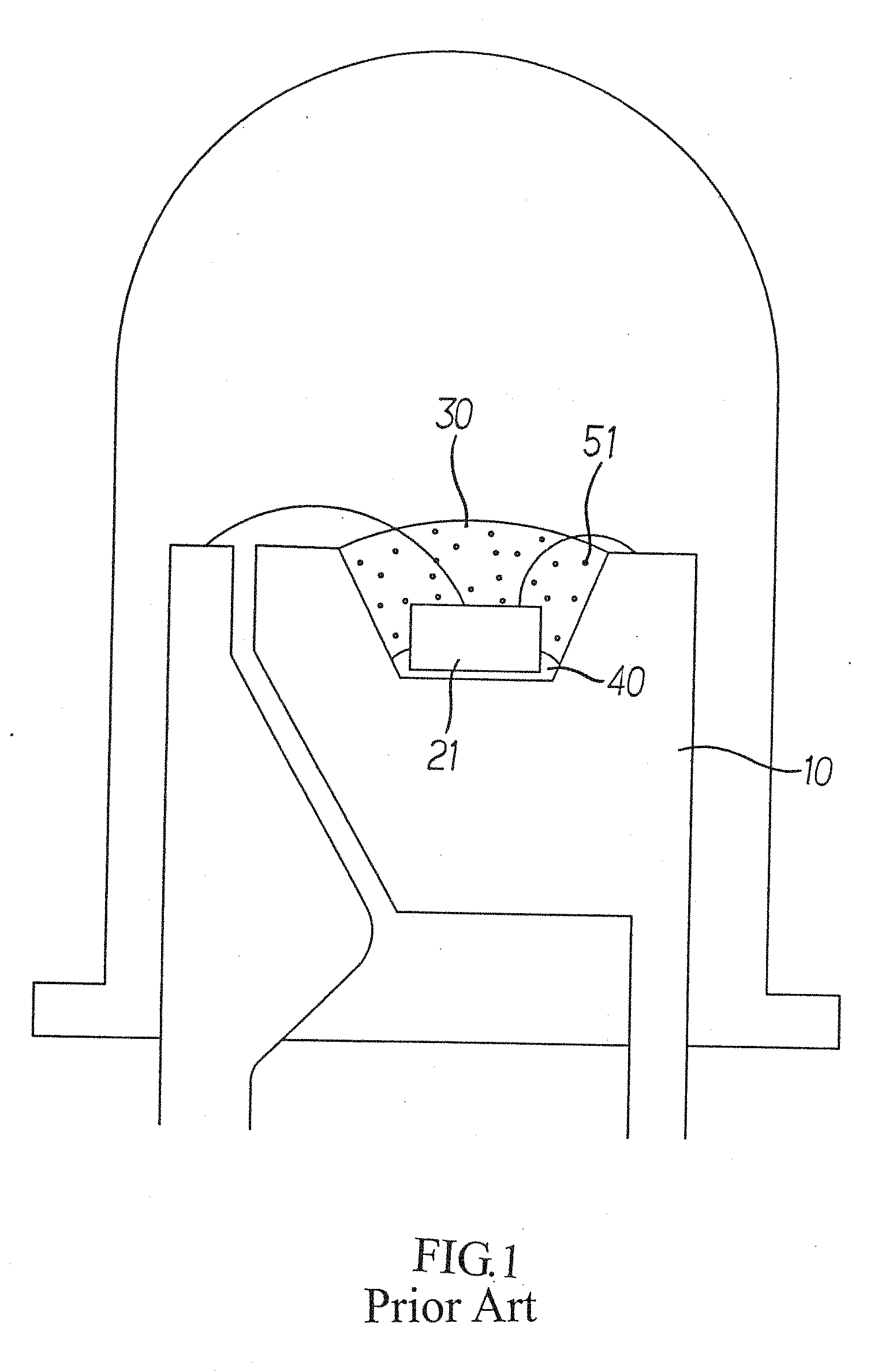
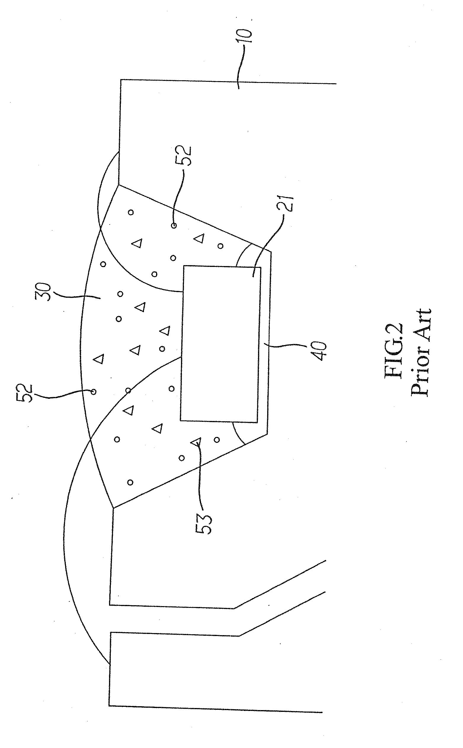
[0019]Referring to FIG. 3, a preferred embodiment of the present invention is essentially having fixed at the bottom of a light emitting chip 20 in a given color a first non-conductive material 61 containing a phosphor 50 in a color corresponding to that of the chip 20. The first non-conductive material 61 is bonded to the bottom of the chip 20 either by the spin coating or baking solidification method to form a die unit for the manufacturing of a white multi-wavelength LED of the present invention.

[0020]Accordingly, the first non-conductive material serves as the position for coating an encapsulating material to secure the die unit onto a carrier. A golden plated wire connects the circuit of the light emitting chip 20 and finally a second no-conductive material containing a phosphor in a color corresponding to that of the chip 20 is injected to cover up the top of the chip 20 to allow light from the chip 20 to pass through both of the first and the second non-conductive materials t...


PUM


Abstract

A white multi-wavelength LED and its manufacturing process has bonded at the bottom of a light emitting chip in a given color a first non-conductive material containing phosphor in a corresponding color to that of the chip to become a die unit; the first non-conductive material functioning as the position where the die unit is bonded to a carrier; golden plated wire constituting the circuit connection of the chip; a second non-conductive material containing phosphor in a color corresponding to that of the chip being injected to cover up the top of the chip to emit the expected white light and effectively promote the luminance performance of the LED.

Description

BACKGROUND OF THE INVENTION[0001](a) Field of the Invention[0002]The present invention is related to a white multi-wavelength light emitting diode (LED), and more particularly to a light emitting diode that emits light of correct color and effectively promotes the performance of luminance, and a manufacturing process of the LED.[0003](b) Description of the Prior Art[0004]Usually a light emitting diode is comprised of having a packaging material (non-conductive material) to wrap up a light emitting integrated circuit (IC), and a golden wire to connect IC electrodes to the circuit so that once the IC is conducted, it emits the light to outwardly irradiate through the packaging material, and the light emitted from the chip is further incorporated with the wavelength of a non-conductive material in the packaging material to emit the light in an expected color.[0005]As illustrated in FIG. 1 of the accompanying drawings of the present invention, a while LED construction of the prior art h...

Claims


Application Information

Patent Timeline
Patent Type & Authority Applications(United States)
IPC IPC(8): H01L33/00
CPCH05B33/04H05B33/10
Inventor LEE, MING-SHUN
Owner LEE MING SHUN
Why Eureka
Try Eureka