Methods of fabricating silicon carbide power devices by at least partially removing an n-type silicon carbide substrate, and silicon carbide power devices so fabricated

a technology of silicon carbide power devices and silicon carbide substrates, which is applied in the direction of semiconductor devices, electrical equipment, semiconductor/solid-state device details, etc., can solve the problems that the quality and conductivity of silicon carbide p-type substrates used to fabricate n-channel igbts are generally lacking, so as to reduce the disadvantages of using p-type substrates or eliminate them

Active Publication Date: 2008-12-04
CREE INC
View PDF20 Cites 103 Cited by
  • Summary
  • Abstract
  • Description
  • Claims
  • Application Information

AI Technical Summary

Benefits of technology

[0012]Some embodiments of the invention fabricate a silicon carbide power device by forming a p-type silicon carbide epitaxial layer on an n-type silicon carbide substrate, and forming a silicon carbide power device structure on the p-type silicon carbide epitaxial layer. The n-type silicon carbide substrate is at least partially removed, so as to expose the p-type silicon

Problems solved by technology

Unfortunately, 4H silicon carbide p-type substrates that would be used to fabricate n-

Method used


Image

  • Methods of fabricating silicon carbide power devices by at least partially removing an n-type silicon carbide substrate, and silicon carbide power devices so fabricated
  • Methods of fabricating silicon carbide power devices by at least partially removing an n-type silicon carbide substrate, and silicon carbide power devices so fabricated
  • Methods of fabricating silicon carbide power devices by at least partially removing an n-type silicon carbide substrate, and silicon carbide power devices so fabricated

Examples


Embodiment Construction

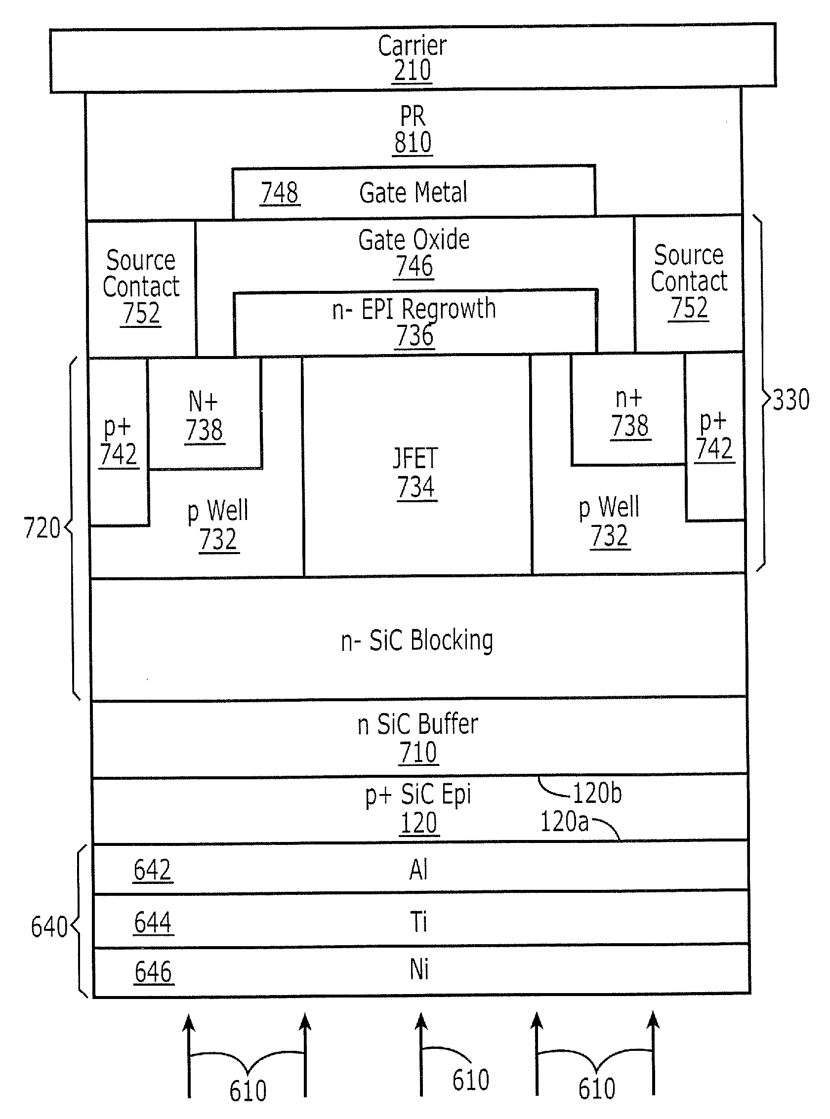
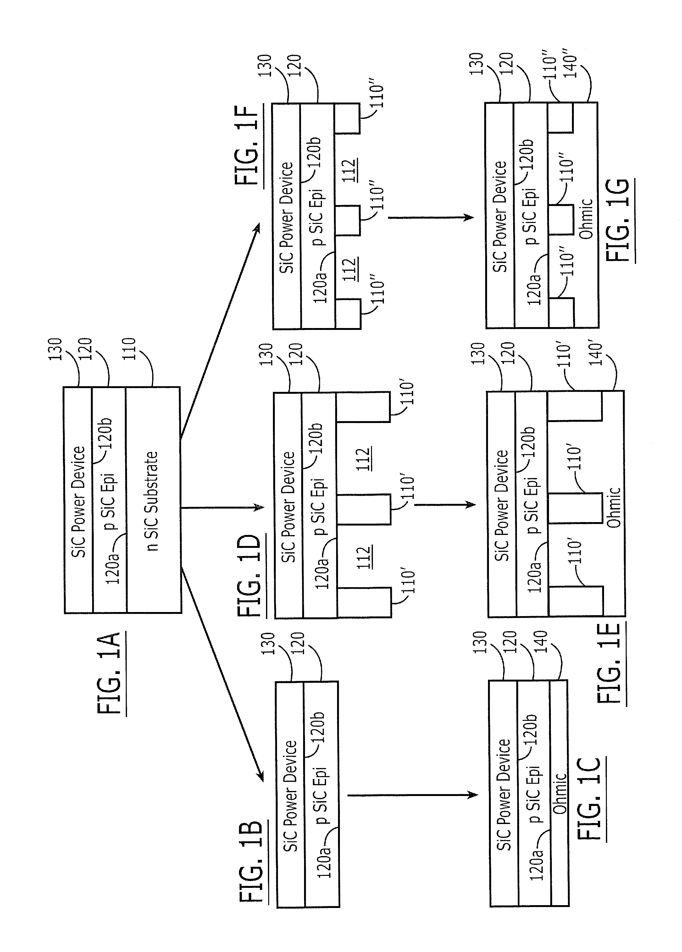
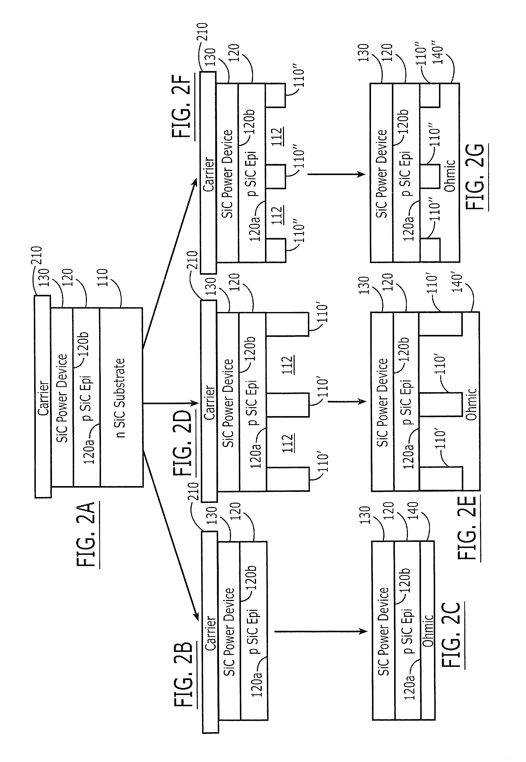
[0026]Embodiments of the present invention now will be described more fully hereinafter with reference to the accompanying drawings, in which embodiments of the invention are shown. This invention may, however, be embodied in many different forms and should not be construed as limited to the embodiments set forth herein. Rather, these embodiments are provided so that this disclosure will be thorough and complete, and will fully convey the scope of the invention to those skilled in the art. Like numbers refer to like elements throughout.

[0027]It will be understood that, although the terms first, second, etc. may be used herein to describe various elements, these elements should not be limited by these terms. These terms are only used to distinguish one element from another. For example, a first element could be termed a second element, and, similarly, a second element could be termed a first element, without departing from the scope of the present invention. As used herein, the term ...


PUM


Abstract

A silicon carbide power device is fabricated by forming a p-type silicon carbide epitaxial layer on an n-type silicon carbide substrate, and forming a silicon carbide power device structure on the p-type silicon carbide epitaxial layer. The n-type silicon carbide substrate is at least partially removed, so as to expose the p-type silicon carbide epitaxial layer. An ohmic contact is formed on at least some of the p-type silicon carbide epitaxial layer that is exposed. By at least partially removing the n-type silicon carbide substrate and forming an ohmic contact on the p-type silicon carbide epitaxial layer, the disadvantages of using a p-type substrate may be reduced or eliminated. Related structures are also described.

Description

STATEMENT OF U.S. GOVERNMENT INTEREST[0001]This invention was made with Government support under Contract No. N00014-05-C-0202 awarded by ONR / DARPA. The Government may have certain rights in the invention.FIELD OF THE INVENTION[0002]This invention relates to methods of fabricating power devices and the resulting devices, and more particularly to silicon carbide power devices and methods of fabricating silicon carbide power devices.BACKGROUND OF THE INVENTION[0003]Power devices are widely used to carry large currents and support high voltages. Modern power devices are often fabricated from monocrystalline silicon semiconductor material. One widely used power device is the power Metal Oxide Semiconductor Field Effect Transistor (MOSFET). In a power MOSFET, a control signal is supplied to a gate electrode that is separated from the semiconductor surface by an intervening insulator, which may be, but is not limited to, silicon dioxide. Current conduction occurs via transport of majority...

Claims


Application Information

Patent Timeline
IPC IPC(8): H01L21/44H01L23/48
CPCH01L21/0475H01L21/0485H01L2924/12032H01L2924/1305H01L2924/13062H01L2924/1301H01L2924/10271H01L21/268H01L2924/01033H01L23/4827H01L29/1095H01L29/66068H01L29/7395H01L2224/04026H01L2924/01013H01L2924/01014H01L2924/01022H01L2924/01078H01L2924/01079H01L2924/10272H01L2924/13055H01L2924/13091H01L2924/01005H01L2924/01006H01L2924/00
Inventor DAS, MRINAL KANTIZHANG, QINGCHUNCLAYTON, JR., JOHN M.DONOFRIO, MATTHEW
Owner CREE INC
Why Eureka
Try Eureka